3d printing
08 Jun 2020

Nano Dimension’s CEO Yoav Stern is talking about new trends to create PCBs

Apr 11, 2019
The latest and greatest evolution in modern manufacturing is additive manufacturing. In contrast to subtractive manufacturing, where system parts are built by removing material from a workpiece, additive manufacturing is used to build up a product layer-by-layer using 3D printing technology. This offers researchers, hardware startups, and established manufacturers many advantages, particularly for designing and prototyping functional electrical and electromechanical parts, opening the door to new possibilities in electronics design and manufacturing.
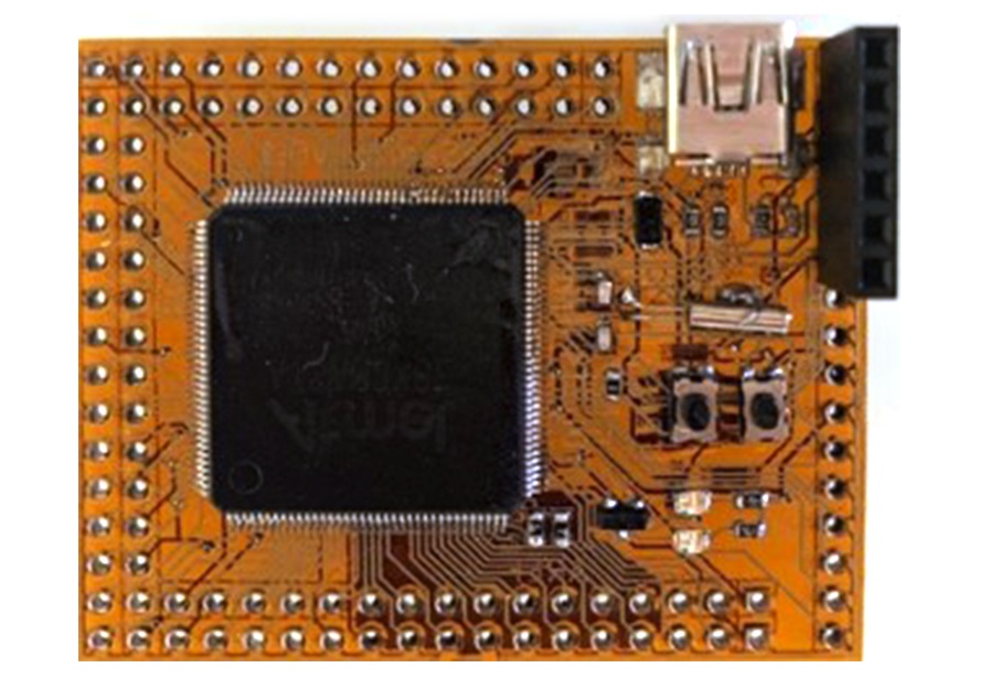
Additive manufacturing allows for the printing of multilayered printed circuit boards.
Additive manufacturing of electronics is not without its challenges, however. Most EDA software is not equipped to design complex 3D and non-planar electronics, forcing designers to default to CAD software to design electronic devices. When designing for additive manufacturing, designers must understand the manufacturing process to tap into the opportunities and account for the limitations of additive manufacturing. This is how to achieve a design that is optimized for 3D printing.
Here are four best practices to help you overcome these challenges and use additive manufacturing for innovative design and production:
When it comes to additive manufacturing, less is more. With design for traditional manufacturing (DFM) or design for assembly (DFA) processes, designers have to worry about mating many separate parts at specific surfaces and bolt holes, accounting for shrinkage during casting or injection molding, and including the appropriate draft angles to eject parts from a mold or cast. In electronics and PCB design, tooling for vias or other fastener holes can be a significant cost driver, as well as the traditional overheads of multilayer fabrication and assembly. All of these elements must be included in your design.
In addition, with DFM, adding layers to your design, which can help decrease board size, comes at significant prototyping and manufacturing cost. When designing complex circuits and antennas, it is very difficult to get the design right the first time, and it takes several iterations and trial and error before you know you’ve created the best design for your specific requirement.
Meanwhile, design for additive manufacturing (DAFM) invites the designer to consolidate parts into a single piece, thus alleviating some design constraints associated with traditional manufacturing. 3D printing can be used to seamlessly print an entire multilayer PCB layer-by-layer rather than traditional etching of individual layers, completely eliminating bonding, drilling, and plating steps. Designers can optimize their designs such that multiple parts are consolidated into single units to the greatest extent possible. Imagine being able to combine a board with a bracket and an antenna all in one part, for example.
With more complicated products, each part can be created separately and later joined within your CAD software. Any portion of the product that will be printed could appear as a single unit in your design software, rather than planning on including fasteners or bonding steps in your assembly process. This will help ensure that your 3D printed circuits, antennas, and other components are both electrically and structurally optimized.
Traditional PCB design and EDA software can be used to easily design a planar PCB without many problems. Top-notch additive manufacturing systems can easily pick out the dielectric and trace regions in your design and start printing your board. However, when it comes to non-planar or 3D electronics, traditional EDA software does not have the capabilities required to design complex, multi-material non-planar devices, even if today’s additive manufacturing systems for electronics can print such parts. This means electrical engineers are very limited when designing a 3D circuit that doesn’t use a traditional PCB layered approach.
Instead of using a mix of traditional EDA and CAD software for non-planar designs, you should use an additive manufacturing system that interfaces directly with CAD software via a plugin. This allows you to design complex 3D prototypes as a single model directly in your CAD software. The ability to create parts that are completely new implementations of plastronics design can lead to groundbreaking products and novel research.
Additive manufacturing techniques can be used to produce a variety of products in virtually any orientation, but the printing orientation can affect the quality and tolerances of the final product. This issue with orientation affects the circularity of fastener holes, vias, curved traces, board shape, metallic elements, and other complex shapes that appear on your device. If you do not have experience working with advanced additive manufacturing systems, this can create problems with tolerances in PCBs, electronic elements, and optical devices that require high precision.
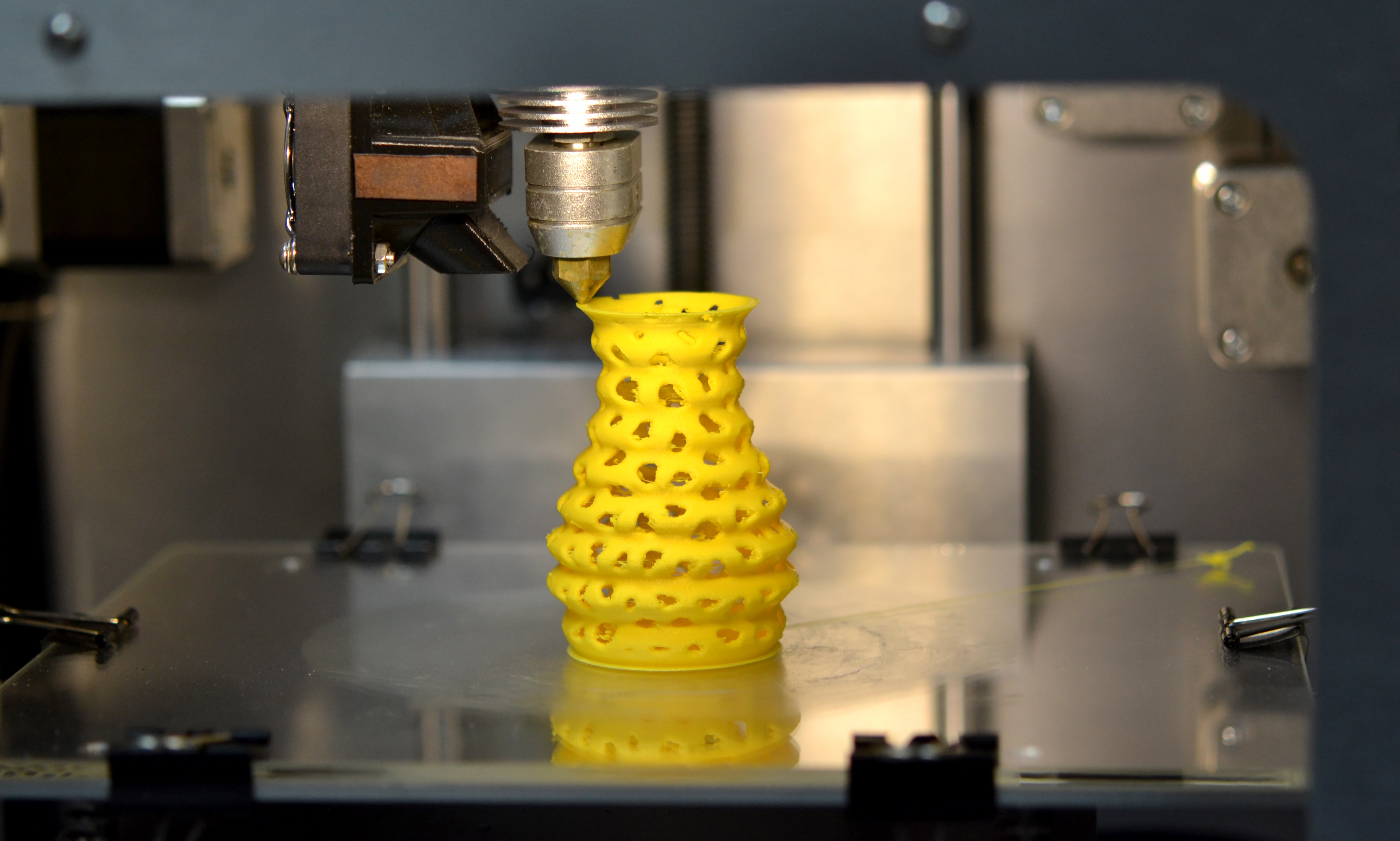
The horizontal plane is the best orientation for printing rounded shapes.
Experimenting with different printing strategies can help you determine the best way to get your device to meet your dimensional specifications. Early adopters of additive manufacturing can benefit by scaling this 3D printing learning curve ahead of the pack.
Just as orientation can affect dimensional tolerances, the X, Y, and Z resolutions of your 3D printer can affect the dimensional tolerances along the printing direction. 3D printers work by depositing material layer-by-layer, and the layer stack is built up vertically. As the printer completes one layer and moves onto the next layer, the print head moves vertically a certain distance and starts depositing the next layer of materials. This vertical distance is called the Z resolution.
The Z resolution determines the minimum thickness of any element that appears on your device. It also determines the allowed thickness of any element on the device. To ensure elements meet your design specifications, the vertical thickness of any element and the vertical spacing between elements should be set to an integer multiple of the vertical resolution. This will also help keep your device within the tolerances specified in your design.
It’s important to note that 3D printers also have X and Y horizontal resolutions that affect the printing accuracy. X and Y resolutions define the feature sizes of a pattern that can be printed in any given layer, such as the line and space measurements of a PCB. This horizontal resolution determines the smallest feature you can print and affects the minimum spacing between elements in a device. Be sure to account for horizontal resolution during the design phase, just as you would the vertical resolution.
When it comes to additive manufacturing for innovative design and production, there are plenty of points to consider. However, following these best practices can help you properly design your next product. From PCBs to antennas to sensors and very complex non-planar electronic circuits, an additive manufacturing system for PCBs can help you build better prototypes and develop theories and technologies that would be impossible to make any other way.
Building an electrically functional prototype for your next electronic device is quick and easy when you use an additive manufacturing system that is tailored for 3D printing and rapid prototyping of PCBs. The DragonFly Pro additive manufacturing system makes it easy to 3D print a functional prototype of your next PCB. If you’re interested in learning more about Nano Dimension’s DragonFly Pro system, contact us today.

Be informed of the future of additive manufacturing &
3D printed electronics

