
Blog
18 Apr 2019

Additive Manufacturing: Advantages and Disadvantages for PCB Prototyping
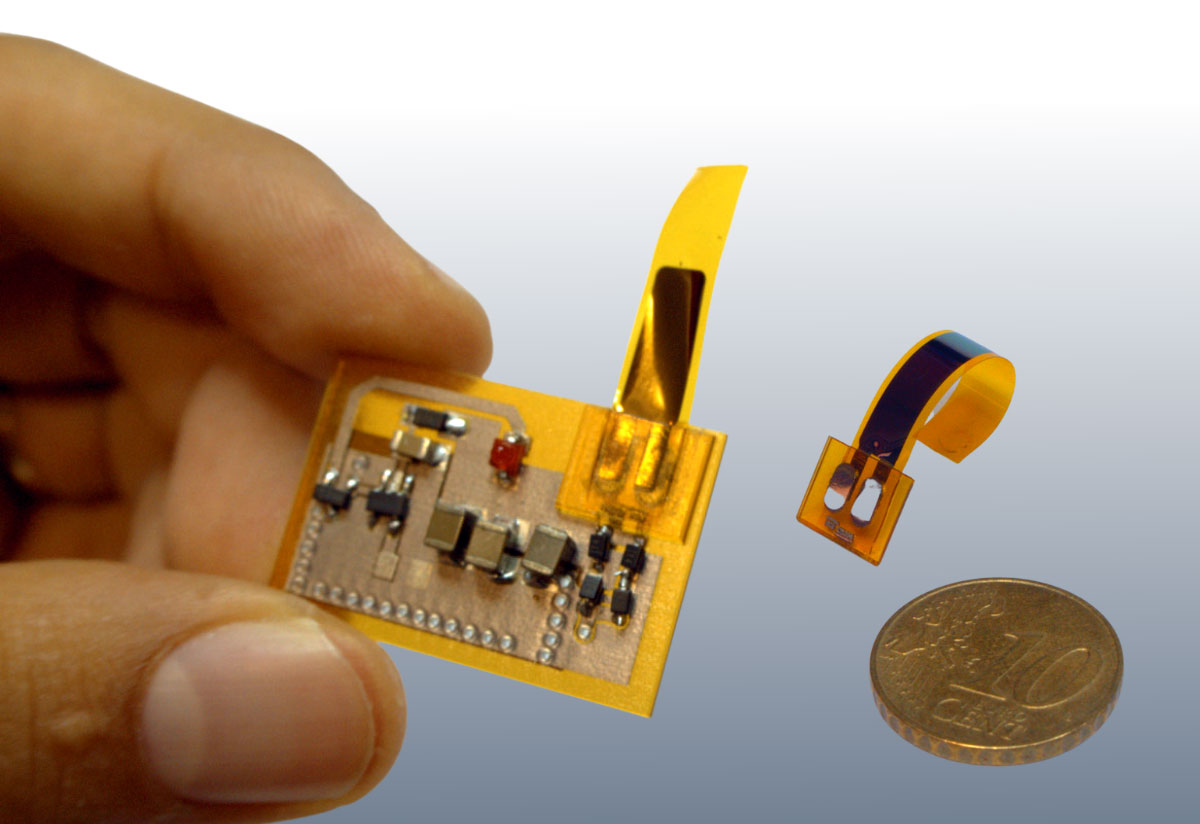
Ever since its introduction in the 1980s, additive manufacturing has steadily become a more prominent method for producing a variety of increasingly complex and demanding prototypes, as well as finished components and products. All it takes is a CAD model and a modest investment in equipment, and even college students can start prototyping from their…