3d printing
08 Jun 2020

Nano Dimension’s CEO Yoav Stern is talking about new trends to create PCBs

Dec 20, 2018
This post was first published by AMFG here. Click here to access Part 1 of the interview.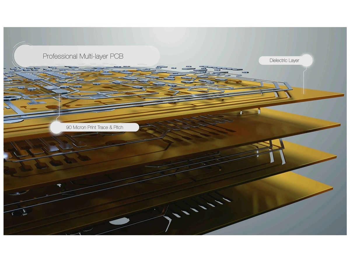
The world of electronics is a young yet burgeoning area for 3D printing. From drones and satellites to laptops and smartphones, electronic devices are playing an ever-greater role in our lives. However, to operate, these devices depend on electronic components such as printed circuit boards (PCBs), antennas and sensors.
3D printing is redefining the way these components have traditionally been designed in part by providing faster product development and greater design complexity, most notably in the area of non-planar (i.e. non-flat) geometries.
 Nano Dimension is a company leading the field of additive manufacturing for printed electronics. Founded in 2012, the Israeli-based company has developed its own technology — the DragonFly Pro System — that can simultaneously 3D print metals and dielectric polymers. Using the technology, companies are able to 3D print prototypes in-house, faster and at a lower cost.
In this week’s Expert Interview, we spoke with Simon Fried, the Co-Founder and President of Nano Dimension, to discuss the rise of 3D printing for electronics and how Nano Dimension is paving the way for this unique application.
A key vertical has been aerospace and defence, with a great example use case being antennas.
When it comes to 3D printing electronics, you can print circuit boards, antennas or parts that are both structural and electrically functional. However, antennas are a bit of a black art: when designing them, you never know exactly how they are going to work. It takes a lot of iterations and trial and error before you know you’ve made the best design that you can for that particular need.
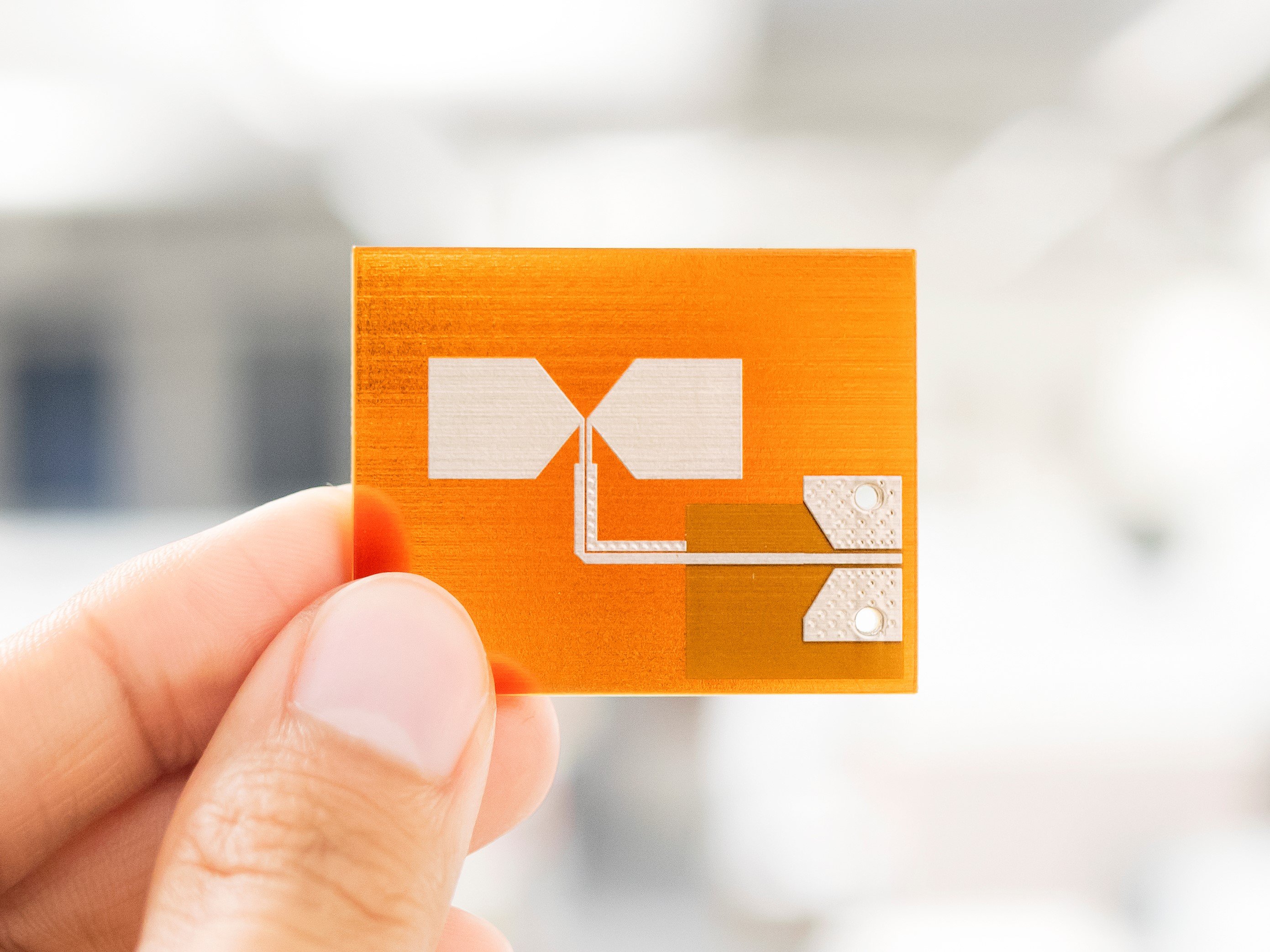
RF Antenna 3D-printed on Nano Dimension’s DragonFly Pro System.
With antennas, we recently worked with a company called Harris Corporation where we achieved quite an exciting breakthrough. Harris wanted to apply the technology to antennas and testing, which wasn’t a use case we’d initially been proposing. Harris helped us to understand that this is a great solution for those who are focusing on designing antennas as well.
More importantly, we found that the 3D-printed antennas performed exactly the same way as traditionally manufactured antennas.
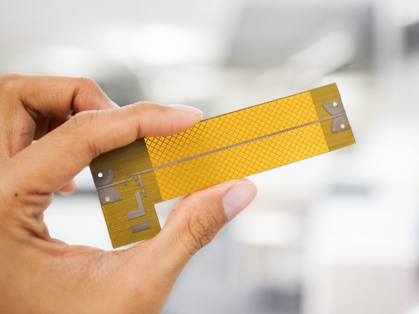
RF Amplifier designed in collaboration with Harris Corporation and 3D-printed on Nano Dimension’s DragonFly Pro System.
So antennas are one application area that is particularly relevant and it falls into that aerospace and defence vertical where low-volume manufacturing of very high complexity items is a key focus. That’s very much a sweet spot of additive manufacturing in general, where you see complexity and low volume.
If you’re looking at production volumes in the of hundreds of millions, then additive manufacturing isn’t the answer in any industry, at least not yet. But it certainly is in the aerospace niche, where there is not so much of a volume question as there is the element of reliability and solving complex problems.
Why has aerospace and defence been such a key vertical? Defence companies need to maintain a great level of secrecy. Another constraint is that they are limited in the number of suppliers that they’re allowed to work with, and their internal procedures for releasing a design file to a third party are incredibly complex. These types of companies have the combination of a need for security and low-volume manufacturing as they’re working on discrete and high-value projects. And that’s really where additive took off, in the mechanical types of application as well. So we are following suit in terms of discovering where the application happens first.
If you want to use our technology to make a traditional green printed circuit board (PCB), one that is square or rectangular and flat, that is the space where you have electronic design automation software.
You have CAD software in the 3D world and in the electrical world you have EDA software, which is software we can work directly with. If you use this software to design a circuit board, our software will essentially interface with traditional design software and print it out. That’s the existing flow, using existing file formats and we don’t require anybody to do anything that that hasn’t been done before.
Where you do have challenges on the software side is when you start looking at what’s called non-planar electronic circuits, essentially creating circuits that are not flat. For example, instead of the green motherboard being a rectangle, it might be a pyramid or cube because that shape fits a particular space in a more optimal way.
When you look at designing 3-dimensional electronics that don’t use the traditional layered PCB flat design approach, electrical engineers today are incredibly limited. They can’t design an electrical trace that is anything other than flat because that’s the way PCBs are traditionally manufactured. And yet it could be really useful if they could design traces that were at an incline. Currently, if a designer wants to do something different, something that frees up a lot of the constraints, such as design non-planar circuitry they will have to use mechanical CAD software, which is really intended for mechanical engineers.
At the moment, while our printers are certainly able to print non-planar geometries, currently there is no EDA software around that is able to design such parts. That’s why we now see large companies like Siemens or Dassault Systèmes looking to integrate the worlds of electrical and mechanical design with their software packages. Nano Dimension has developed an add-in to SolidWorks that integrates directly to our precision 3D printing system.
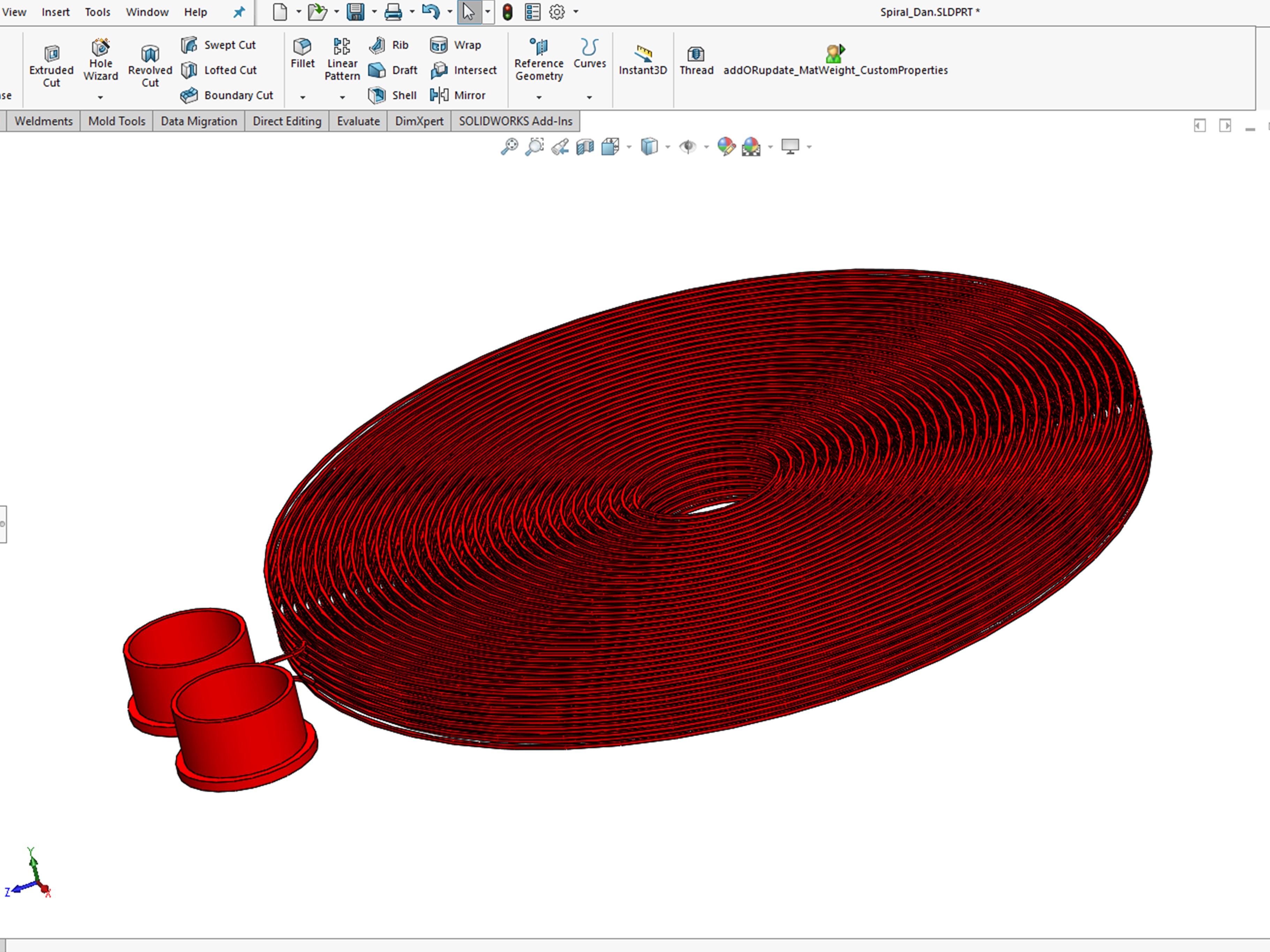
An electromagnet designed for additive manufacturing on Nano Dimension’s DragonFly Pro System, as visualized on SolidWorks using the Nano Dimension Add-in.
We’ve seen the same trajectory with traditional 3D printing as well. If we go back a decade and ask people which CAD software they were using to design full-colour parts, the software wasn’t necessarily able to facilitate such designs. Even though there were certainly printers out there able to deposit colours in ways that would have made it physically possible to print, just very difficult or perhaps impossible to design.
There are things in the electrical space that are like that as well, where the printer can certainly print, but we may have to wait a few years before the features in the design software are actually developed.
Yes, very much so. Particularly, in the non-flat area. Non-planar, new geometries require new design software which is waiting in the wings.
Additive manufacturing faces the challenge of not succumbing to the second wave of hype. We all know about the big 3D printing bubble around 2010, which was driven by hype and over—expectation, with the industry getting caught up in its own narrative. And now what we’re seeing is a kind of a replay of that with people using the term additive manufacturing instead of 3D printing.
So the question is will the systems really start to deliver in time for this not to be seen as yet another wave of hype? That’s a risk for everybody in the industry. Can the technology continue its transition to manufacturing?
Certainly, additive manufacturing is now much readier to play a manufacturing role, so it’s often a question of what role it will play as a business tool. It used to be just a time-compression prototyping tool but now AM is a technology for organisations to adopt just as they would any other manufacturing technology. What we are seeing is different types of additive manufacturing systems being integrated into traditional manufacturing lines. The role is shifting from the early design stages to either complementing manufacturing by producing jigs and test-fixtures or by actually producing final parts.
On top of that, the additive manufacturing industry definitely needs solutions to more materials. 3D printing is theoretically capable of producing parts of high complexity and functionality, whether it’s mechanical, biological, electrical. But making that happen comes down to having enough material options. Polymers are getting stronger, a wider range of metals is now printable and for electronics additional functional aspects such as dielectric constants are paramount.
Along with materials, there’s also the question of standards. To properly mature as an industry, you need to have standards that everybody subscribes to. You need to have processes, like ways of tracing products and ensuring IP protection for files. So for the industry, it will be less of the glitz and glamour and more of the nuts and bolts of how to deploy these technologies effectively.
I have a reasonable amount of hope as more and larger companies are engaged at this time and we’re seeing actual strategies in place rather than just excitement. So I think yes, there are enough big companies and enough experienced people in the industry now, that it will rise to the occasion. So yes, it’s a big opportunity not without its challenges. I think the additive manufacturing industry will deliver on its promise.
For a company that has no or little knowledge of AM, my recommendation would be to understand that manufacturing of this type is a non-trivial consideration. It’s a complex space with many different types of printers, materials and so on. The technologies you decide to explore and try out may well not be the right ones.
So one needs to be very informed of exactly what one wants to do and be prepared for a learning curve — often the engineers who get the system don’t necessarily have a deep understanding of how to deploy it. We certainly recommend people learning more, they should engage with service bureaus earlier rather than later and start to get their head around what the different technologies are and service bureaus are a phenomenal way to understand what the offerings are and how different deposition technologies and materials actually deliver to the needs of your organisation.
There are a lot of opportunities and one is best served by exploring them in a methodical way and being willing to learn.
So plan ahead of time, use service bureaus, understand the huge differences between the different approaches. There is no such thing as “additive manufacturing”, it’s really which material and which machine are best for your particular application.
We hope 2019 will be as great a year for us as 2018. While I can’t really comment on specifics, we’ll continue to launch our technology as we have been doing this year. Overall, we’re very confident that additive manufacturing of electronics will be as well received as additive manufacturing of mechanical parts — and perhaps even more so!
This post was first published by AMFG here.

Be informed of the future of additive manufacturing &
3D printed electronics

