3d printing
08 Jun 2020

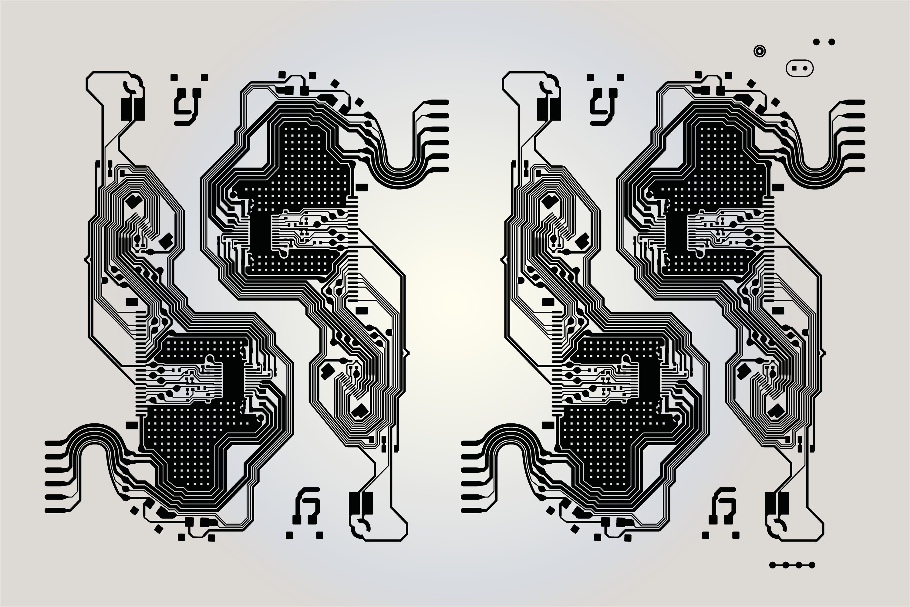
Nano Dimension’s CEO Yoav Stern is talking about new trends to create PCBs

Dec 19, 2019
 IoT devices, new mobile devices, UAVs/UUVs, unique systems in aerospace and defense—all of these products and many more now require wireless communication in one or more frequency bands, often simultaneously. This means each of these systems will need one or more antennas to operate in their intended environments. This is in addition to the large number of other components these devices require to work properly.
With form factors in many advanced products becoming more demanding and miniaturization being a constant trend in electronics, designers should consider unique ways they can reduce component count while optimizing for communication in a variety of frequency bands.
Rather than depositing multiple planar antennas or using multiple COTS antennas, designers can meet their form factor and functionality requirements by designing a nonplanar antenna on a PCB substrate with complex shape. Traditional PCB manufacturing systems have made this very difficult, but creating this type of structure becomes quite simple when you work with the right additive manufacturing system.

You can recreate these phased arrays as a nonplanar antenna with complex geometry using a 3D printer.
A nonplanar antenna is effectively a microstrip or patch antenna that is deposited on a curved substrate. As nonplanar antennas must be deposited on nonplanar surfaces, their use in PCBs is rather difficult. Standard planar laminates cannot be used unless they are built into molded interconnect devices, which essentially form an odd array of planar antennas. Standard antenna designs can be easily adapted as nonplanar devices by depositing them on a flexible substrate material and forming the substrate to the desired geometry. Although this is an easy way to adapt a standard nonplanar antenna into any desired shape, there is a risk that the conductors will fracture while forming the antenna.
Flex ribbons in rigid-flex PCBs can be used to support a nonplanar microstrip antenna with standard geometry, allowing the substrate to be curved along one dimension and molded to another rigid surface. The rigid portions of the board can then hold other components and a transceiver to drive the device. Other nonplanar antennas are effectively aftermarket components—they can be pasted or molded to a curved surface and connected to a PCB with a small coaxial cable (e.g., 105263 and 146234 series).
Nonplanar antennas are not a new idea. Research into this topic has been funded by governments over the last decade. Two examples include nonplanar GPS antennas and nonplanar phased array antennas. These antennas can be fabricated on traditional flex substrates (e.g., polyimide) or on a molded interconnect device using standard PCB processes, but they are confined to flat geometry if placed on a rigid PCB substrate due to difficulties in substrate forming, etching, and plating on standard PCB laminates.
One interesting direction with phased array antennas is to place arrays on a curved substrate, which would allow the directionality to be uniquely swept throughout a range of angles along the curvature of a substrate. Contrast this with an array confined to a planar substrate, which only allows transmission at a single angle at a time. This can be done with a curved solid substrate or a flex substrate. In either case, designers need to consider how impedance matching conditions change as the substrate is bent. Working a nonplanar antenna on a flex substrate requires over-forming the substrate so that impedance matching conditions do not change during operation.
Fractal antennas have been widely used in mobile handsets as wideband/multiband antennas. These antennas consist of repeating elements that are printed directly on a planar substrate. In contrast to a typical dipole antenna, the mode structure of these antennas can be tailored by choosing the appropriate size of repeating shape in the fractal, as well as the scaling factor. These antennas can be easily modeled with standard simulation software, but their use has been limited to planar PCB substrates.
Many unique and upcoming applications, such as defense, aerospace, 5G cellular devices, and other beyond-mmWave applications can benefit from a fractal antenna as it reduces the total device count while allowing the resonance structure to be tailored for use in specific frequency bands. Placing these antennas on a nonplanar substrate is a natural next step for tailoring the directionality of these antennas and for investigating new fractal structures for wideband/multiband antennas for mmWave and higher frequencies. While these and other applications are difficult to reach with standard PCB manufacturing processes, an additive manufacturing process can be used to easily fabricate these complex antennas.
The difficulties in forming nonplanar antennas on traditional PCB substrates can be solved by working with an additive manufacturing system. Many possible processes can be used to deposit conductive traces on a planar substrate, such as FDM. However, aerosol jet and inkjet processes are superior for nonplanar antenna fabrication as it allows co-deposition of a substrate and conductors in a single layer-by-layer process. This enables the antenna to be built up on a substrate with any geometry.
This complex flexible geometry can be easily deposited with an inkjet 3D printing process.
The substrate itself can also be built up with a nonplanar geometry using an inkjet deposition process. The layer-by-layer inkjet deposition process doesn’t limit designers to a standard orthogonal interconnect structure—designers can innovate any interconnect structure requires to support a nonplanar antenna, including on a multilayer board. This type of nonplanar structure with arbitrarily curved antenna elements is nearly impossible to accurately manufacture with standard PCB plating and etching techniques.
As the range of available insulating and semiconducting materials for use in additive manufacturing systems continues to broaden, planar and nonplanar antenna designers will be able to optimize channel dispersion, parasitics, and dielectric losses for specific frequency bands, making different nonplanar antenna geometries and specialized substrate material ideal for advanced applications. Designers that are looking seriously at integrating nonplanar antennas into their new products can create fully functional electronics with these unique antennas using an additive manufacturing system.
If you’re developing advanced electronics and need to produce new designs with a variety of embedded components, you need a powerful additive manufacturing system for producing PCBs with planar or non-planar geometry. The DragonFly LDM system from Nano Dimension is ideal for high-mix, low-volume production of complex PCBs in-house. You’ll be able to produce unique PCBs with embedded components, nonplanar antennas, and other innovative devices. Read a case study or contact us today to learn more about the DragonFly LDM system.

Be informed of the future of additive manufacturing &
3D printed electronics

