3d printing
08 Jun 2020

Nano Dimension’s CEO Yoav Stern is talking about new trends to create PCBs

Oct 24, 2019
Like many technical industries, the list of acronyms used to describe additive manufacturing processes and tools is extensive and will only grow over time. Among the long list of commercialized processes and those still in the research phase, inkjet printing is particularly unique for its adaptability and efficiency in printing fully functional products. The range of materials that can be used in inkjet printing and related processes is broad, allowing these systems to be used for additively manufacturing a variety of mechanical or electrical products.
The 3D inkjet printing process is similar to other 3D printing processes in that it proceeds through layer-by-layer deposition. Printing instructions in each layer are generated from a 3D mechanical model for your product, just as is done with popular fused deposition modeling (FDM) systems. However, this established additive manufacturing process is unique in that it is adaptable to a wide range of liquid materials or solid suspensions, providing conductive or insulating structures with high printing resolution. Compared to processes that involve the fusion of metal or plastic materials, inkjet printing requires no post-processing—the finished printing product will be fully functional as soon as it leaves the printing system.

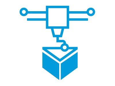
A 3D inkjet printing process can be used to print electronics with any geometry.
3D inkjet printing is a low-temperature, low-pressure process that involves the deposition of liquid materials or solid suspensions. Polymers, dielectric nanoparticles, and conductive nanoparticles can be deposited with this process, making it adaptable to a broad range of materials. In this process, the printing material is extruded through a small nozzle within a print head. As the print head raster scans over a surface, multiple layers are built up in a layer-by-layer process.
Each deposited layer must be cured in between successive depositions, and the curing process will vary depending on the materials used to print your product. Inkjet 3D printing systems include equipment for curing each layer within the system. While the need to cure each deposited layer in between depositions may sound time consuming, the deposited layers are very thin and can be cured quickly, ideal at low temperature or with an optical process (such as exposure to infrared or ultraviolet light).
Printing resolution is an important parameter in any 3D printing system because this determines the smallest feature sizes and tolerances that can be reliably deposited with your system. The limiting factors that determine in the 3D inkjet printing process are the droplet size, which is determined by the size of the nozzle in the print head. In general, a smaller nozzle will provide a higher resolution (i.e., smaller printed features). The 3D inkjet printing process provides high-resolution conductive and insulating structures with a broad range of materials, making it ideal for additively manufacturing advanced PCBs with high interconnect density and high layer count.
Similar to other 3D printing processes, inkjet printing is complexity agnostic, meaning the printing time is nearly independent of product complexity. The time required to print a fully functional product depends solely on the time required to deposit the necessary amount of material and the curing time.
As a result, the cost structure only depends on the weight of the material being deposited and the energy consumed during deposition—costs in both of these areas are fixed. When printing complex multilayer and non-planar PCBs, all interconnects, mounting holes, and vias can be printed directly without additional machining steps. This reduces the total manufacturing time from weeks to hours with a highly predictable cost structure.
Once the printing process concludes, the finished product does not require any further post-processing. Contrast this with other processes, such as FDM, selective laser sintering, and powder bed fusion. These processes involve extrusion of molten materials through a print head, and the printed products tend to have some defects and ridges on the outer surface.
Producing electronics and PCBs with a 3D inkjet printing process requires working with a conductive nanoparticle suspension for printing traces, as well as an insulating polymer for printing substrates. The use of conductive nanoparticles in an inkjet process carries several advantages for use in electronics, but these materials are ideal for 3D printing PCBs with an inkjet process. When combined with the appropriate insulating polymer, you’ll have the materials required to print fully functional PCBs with a 3D inkjet printing process.

Multiple materials can be printed with the right 3D inkjet printing system.
The 3D inkjet printing process is highly adaptable to several materials that can be deposited and cured at relatively low temperature and ambient pressure. As liquid inks are extruded through a nozzle in this process, the system parameters (such as deposition pressure and temperature, as well as curing parameters) can be easily tuned to accommodate materials with different viscosities and curing requirements.
When 3D printing PCBs, there are several points to consider when selecting materials and the appropriate deposition system. Inkjet printing is unique compared to solid-state deposition processes in that it can be used for co-deposition of an insulating substrate and conductive elements simultaneously. As the range of available materials for these systems expands, the market should anticipate 3D inkjet printing of semiconductor devices and a variety of substrate materials that are ideal for operation in different frequency bands.
If you want to use the 3D inkjet printing process for the fabrication of complex PCBs, then you need an inkjet system that provides co-deposition of insulating and conductive materials with high throughput. The DragonFly LDM additive manufacturing system from Nano Dimension is ideal for in-house PCB prototyping or full-scale fabrication of complex electronics with a planar or non-planar architecture. Read a case study or contact us today to learn more about the DragonFly LDM system.

Be informed of the future of additive manufacturing &
3D printed electronics

