3d printing
08 Jun 2020

Nano Dimension’s CEO Yoav Stern is talking about new trends to create PCBs

Jun 20, 2019
 PCB manufacturing is due for an upgrade. The processes used to manufacture multilayer PCBs have remained largely unchanged ever since they were industrialized. The standard multilayer PCB manufacturing process is still as inefficient, wasteful, and prone to errors as it was when it was first adopted by industry.
With the dawn of Industry 4.0 and continuous innovation of additive manufacturing systems and processes, electronics designers and manufacturers have real opportunities to create complex multilayer PCBs for new electronics products with unique architectures, geometries, and capabilities. Realizing such advances is unwieldy or impossible with the traditional multilayer PCB manufacturing process. With the right additive manufacturing system, you can bring fabrication in-house and produce more densely populated boards which allows miniaturization and development of complex devices with advanced capabilities at competitive costs.
Soldering: just one aspect of the multilayer PCB manufacturing process
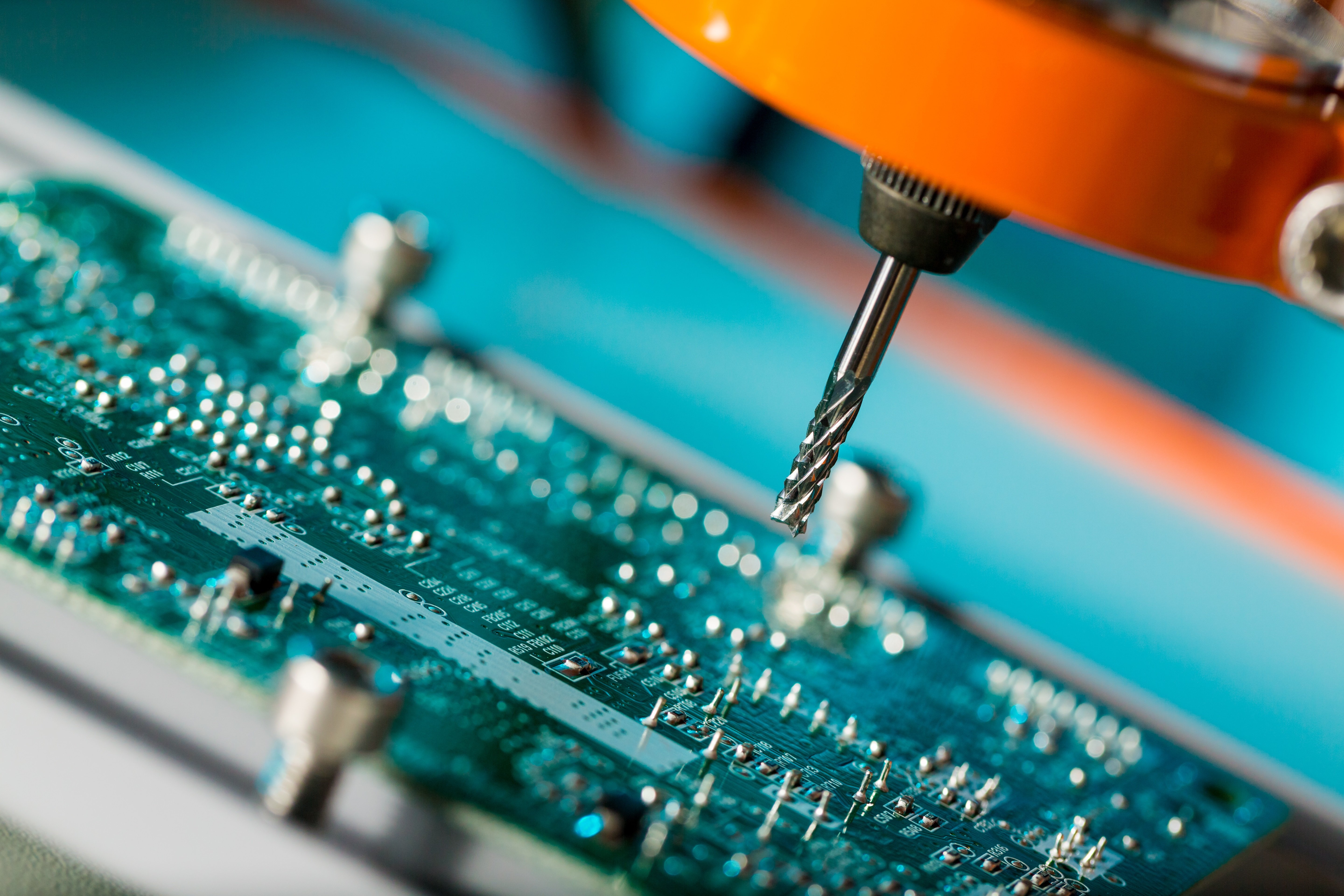
If you’re familiar with the multilayer PCB manufacturing process, then you know that it is a process that has been used since the 1950s. PCB manufacturing, especially multilayer PCB manufacturing, is one area that has lacked significant automation over the past several decades compared to manufacturing in other industries, making it time-consuming and costly.
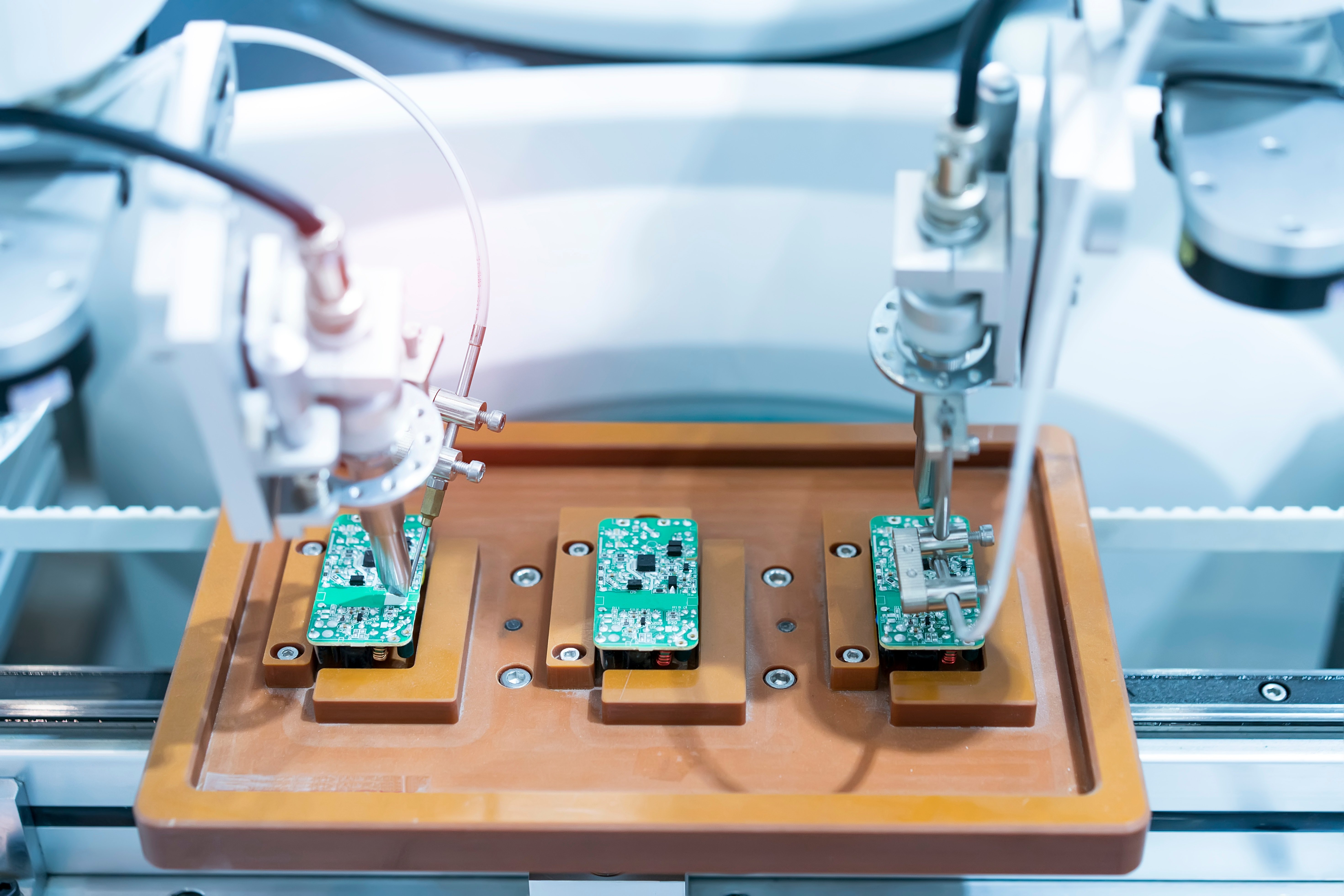
Fabricating a single board requires dozens of repetitive deposition, etching, drilling, and pressing steps. If you are fabricating a PCB that uses a sophisticated routing architecture, such as high-density interconnect (HDI), every-layer interconnect (ELIC), or vertical conductive structures (VeCS), the fabrication difficulties, time, and costs only increase. The result is lower board yield from all but the most specialized manufacturers.
Traditional multilayer PCB manufacturing also involves the use of hazardous chemicals and incurs a significant amount of material waste. These chemicals can cause environmental damage, which is one reason multilayer PCB manufacturing is typically sent overseas. While this makes overseas manufacturers more competitive from a purely cost standpoint, you put yourself at risk of quality defects and counterfeit parts or components. You also risk a bad mark on your company’s image should your overseas manufacturer have very public health and safety problems.
Given these risks associated with the traditional multilayer PCB manufacturing process, electronics designers can benefit from using cutting-edge additive manufacturing systems that are tailor-made for 3D printing electronics.
The application of additive manufacturing processes is challenging the traditional view of multilayer PCB design and manufacturing. In contrast to the traditional multilayer PCB manufacturing process, an additive manufacturing system that is specialized for 3D printing of PCBs produces a multilayer PCB with a single layer-by-layer printing process. In terms of working with an additive manufacturing system, this really challenges the very idea of a “multilayer PCB.”
One additive manufacturing process involves printing conductive traces from silver or copper nanoparticle inks directly onto a rigid FR4 substrate. This essentially eliminates unnecessary subtractive etching steps involved in placing conductive traces on a rigid substrate and works great for printing conductive traces on the surface layers of a single-layer or two-layer board.
When this process of depositing conductive inks on a rigid substrate is applied to multilayer PCBs, this process still carries all the drawbacks of the traditional multilayer PCB manufacturing process. This still requires impregnation and pressing multiple board layers into a complete stackup with the same number of assembly steps as a typical multilayer PCB, providing only minimal cost and time savings.
As 3D printing systems, deposition processes, and available materials have advanced, even more steps in the traditional multilayer PCB manufacturing process have been eliminated. Cutting-edge inkjet printing systems involve just a single layer-by-layer deposition process.
In this process, conductive elements and crucially also the insulating substrate can be printed simultaneously without requiring the pressing of multiple board layers into a single stack. This leaves surface finishing and component placement as the final assembly steps. Drilling steps are completely eliminated as the substrate can be printed with mounting holes, and conductive vias can be printed directly.
The traditional multilayer PCB manufacturing process will eventually go the way of the dinosaur.
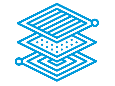
Multilayer PCBs fabricated with this type of additive manufacturing process are not really multilayer at all. Instead, these devices contain embedded traces and vias in a single dielectric layer. This act of embedding conductors actually eliminates the geometric constraints that are normally present in rigid substrates for traditional multilayer PCBs. The substrate can be printed with non-planar geometry as it is not fabricated from successive stacking of planar boards.
Additive manufacturing is currently finding its place in two areas of electronics manufacturing: low-volume, high-complexity production and rapid prototyping of complex electronics. With layer counts in PCBs for newer electronics continuing to increase, topping dozens of layers in extreme cases, an additive manufacturing system is a natural choice for complementing traditional PCB manufacturing capabilities and for rapid prototyping of complex electronics.
In addition to the geometric freedom afforded designers and engineers, using an additive manufacturing system for fabrication of multilayer PCBs makes sense from a business standpoint. Using a 3D printing system that is specialized for PCBs can be used to produce complex multilayer boards with reduced production time, less material waste, and competitive costs. This provides a higher throughput of low-volume, high-complexity electronics.
The reduced manufacturing time for highly complex multilayer PCBs makes additive manufacturing ideal for rapid prototyping of new electronic devices. Keeping this digital manufacturing system in-house eliminates the risks that come with sending a prototyping run overseas, keeps you cost-competitive, and allows immediate testing of finished prototypes. This hastens the overall R&D process and helps you get to market much faster.
Now you can bring rapid prototyping capabilities in-house when you use the DragonFly Pro additive manufacturing system from Nano Dimension. This unique additive manufacturing system is reinventing the multilayer PCB manufacturing process. You’ll be able to quickly digitally manufacture multilayer boards with complex architectures with lower cost and faster production time. Read a case study or contact us today if you’re interested in learning more about the DragonFly Pro system.

Be informed of the future of additive manufacturing &
3D printed electronics

