Mar 12, 2019

A Brave New World: New Designs and New Options

By Simon Fried, Nano Dimension 


                                     World image with RF antenna and sensor                                     

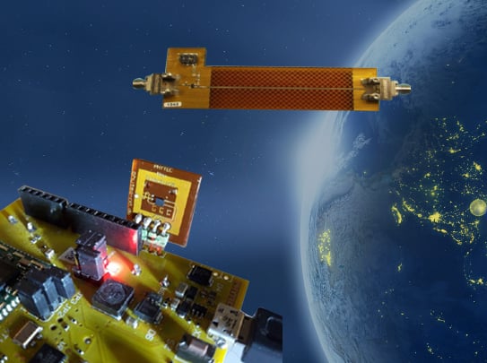
World image with RF antenna and sensor. Source: Nano Dimension


Building functional electronic components in a single print job using inkjet printers with conductive and dielectric inks is transformational in accelerating electronics development and arguably one of the most important breakthroughs for additive manufacturing in the last decade. But as big an engineering feat as that is, there are plenty of other benefits surrounding additive manufacturing for printed electronics.

Here are some of the other highlights:

  • Better Parts

The ability to use precision 3D printing and special functional inks means designers have the flexibility to produce more complex and compact parts, delivering greater part value.

  • Creative Solutions
    • Designing with multiple materials in a single print job allows for far greater design freedom and creativity. That may include, for example, reducing the numbers of parts or combining electrical and mechanical functionality. Designers also can try new shapes for circuit boards because they’re not subject to the limitations of the prototyping facility, which translates into options that can and will impact the size and look of the final products.
  • Less Waste
    • As companies work at becoming more eco-friendly, additive manufacturing provides the strong benefit of creating almost no waste – the printer prints only what is needed. The additive process doesn’t require etching, plating or drilling hich saves on materials expenses and means less waste going into landfill.
  • New Tools for a New World
    • While traditional electrical design software (EDA) is designed for 2D applications, vendors are building 3D CAD software specifically for 3D printing that helps developers simplify design preparation, processing and production while eliminating some of the time-consuming processes of using software automation.
  • IoT Readiness
    • As more and more sensors and other electronic components are embedded into devices spanning the most far-flung reaches of networks – in the Internet of Things — designers are tasked with finding ways of reducing the size and complexity of these “things” all while increasing their functionality. Additive manufacturing for printed electronics opens the doors for designers to consider many more options around the shape and size of “things.”
  • Creating Non-Planar Circuitry
    • This gets back to the increased design options and creativity aspect for designers. Traditional planar circuits are essentially a series of 2D circuits stacked atop one another and connected to each other by drilled and plated interconnects. in contrast, non-planar circuits can have conductive traces going in any direction, without needing traditional layering. Additive manufacturing allows designers to create non-planar parts, paving the way for the creation of things that previously were unmakeable.

In addition to all of these are the well-documented benefits of additive manufacturing for printed electronics: better protection for intellectual property, saving time by sidestepping off-site (often overseas) prototyping, and saving money. If your company is interested in learning about the benefits of additive manufacturing for electronics, contact us by clicking here


Stay Updated

Be informed of the future of additive manufacturing &
3D printed electronics