3d printing
08 Jun 2020

Nano Dimension’s CEO Yoav Stern is talking about new trends to create PCBs

Sep 17, 2019
 Engineers and designers have repeatedly faced and overcome plenty of PCB design challenges. Increasing performance demands in a number of products and industries have forced designers to come up with new ways to pack greater functionality into a smaller footprint. Between innovations in PCB manufacturing processes and innovative design choices, many designers have been successful in keeping up with the demand for greater functionality in a variety of industries.
3D printing has been around for decades, but advances in printing technology have enabled this unique manufacturing process to be applied to additive manufacturing of PCBs and other complex electronic devices. The layer-by-layer printing process provides design engineers with the opportunity to address several unique PCB design challenges in many application areas. It also gives designers the freedom to implement unique architectures in their devices that are not manufacturable with traditional processes.

This routing architecture can be a significant PCB design challenge that can be solved with 3D printing.
Inkjet additive manufacturing systems that can co-deposit conductive and dielectric nanoparticle inks are ideal for fabricating fully functional, high-frequency devices. The dielectric constant for many polymer materials is lower than that of FR4 substrates (ranging from ~4 to ~4.7), and these materials can have a lower loss tangent at higher frequencies. This makes these materials preferable to FR4 and competitive with more expensive high-speed laminates.
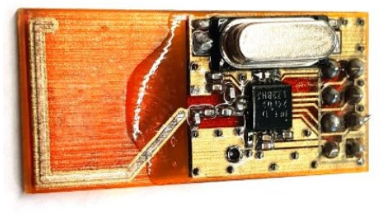
3D-printed RF transceiver
As more devices start operating in high-frequency bands (e.g., in 5G and automotive), the corresponding wavelength will become small enough that it is similar to the size of conductive features that appear in many PCBs. Parasitics also cause greater crosstalk and noise coupling at higher frequencies. This has motivated the use of different and layout routing architectures (e.g., grounded coplanar waveguides) in certain applications.
One challenge at higher frequencies is printing multilayer PCBs to suppress resonance in an insulating layer between two conductors, which can radiate strongly at high frequency. To suppress this type of resonance, the layer thickness needs to range from one-eighth to one-quarter of the wavelength in the substrate. An inkjet 3D printer is ideal for fabricating a multilayer PCB with such a small layer thickness with faster fabrication time and lower cost.
As modern products have continued to pack greater functionality into a smaller package over time, continued miniaturization has always remained a PCB design challenge. The semiconductor industry continuously addresses the demand for greater miniaturization, but other innovations have happened at the PCB level. HDI routing, microvia and other via architecture in boards with high layer count, and selection of components with smaller footprint are common methods to reduce PCB size.
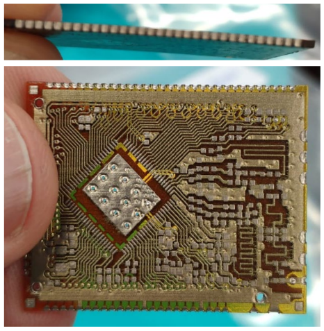
Vertical integration of semiconductor integrated circuits, where ICs are successively stacked vertically and extend into the substrate, is extremely difficult in traditional PCB substrates. Doing this with a subtractive manufacturing process on rigid FR4 or other substrates requires removing portions of the substrate between plating, etching, and pressing operations. This adds to the dozens of fabrication steps for multilayer PCBs.
The layer-by-layer printing process in additive manufacturing already allows fabrication of complex PCBs, where fabrication time and cost structure are nearly independent of device complexity. This allows fabrication of PCBs with vertically integrated ICs, providing a smaller device footprint compared to the same device on FR4. This same procedure allows other components to be embedded in a 3D-printed PCB with negligible increases in the number of fabrication steps.

3D-printed PCB for vertical integration of ICs
Traditional manufacturing of plug-in carrier boards requires many assembly steps. These multilayer boards require through-hole vias to route signals throughout the module and to provide the power, ground, and shielding planes in the internal layers. Assembly requires soldering of mounting pins on the side of the board in addition to the standard multilayer PCB manufacturing steps. Fabrication of these boards is normally outsourced, which carries long lead times. With devices that will appear in strategically sensitive equipment, there is always a risk of intellectual property theft or tampering.
Using an additive manufacturing system to fabricate an SOM eliminates the need for through-hole vias as interconnects can be run between specific layers. This eliminates drilling steps, material waste, and helps ensure signal integrity by reducing inductance on interconnects. The side-mounted pins can also be printed directly on the edge of the board, rather than being soldered. As we will see below, the modified cost structure in additive manufacturing allows the fabrication of these devices to be on-shored, which allows a manufacturer to exert greater control over product quality and security.
Fabrication of an SOM via additive manufacturing makes it so through-hole vias aren’t necessary and allows for side-mounted pins to be printed on the board edge.
In addition to solving the unique design challenges outlined above, using an additive manufacturing system for 3D printing of PCBs provides several other benefits. Products manufactured with traditional subtractive processes must pass a design for manufacturing (DFM) check before they can be approved for production. In contrast to traditional PCB manufacturing processes, the layer-by-layer 3D printing process does not change with device complexity. This gives engineers the freedom to craft unique solutions to complicated PCB design challenges and also develop miniaturized products because they are not constrained by manufacturing processes.
Additive manufacturing processes carry a different cost structure than traditional subtractive processes. This cost structure is nearly independent of device complexity, in part because the fabrication time only depends on the amount of material used in a board, rather than the board’s complexity. The fixed fabrication time and cost structure make additive manufacturing the best option for fabricating low-volume runs of multilayer PCBs with complex geometry.
The change in cost structure and fabrication time arises due to the elimination of redundant assembly and fabrication steps that are required when manufacturing multilayer PCBs. This gives businesses greater predictability when planning manufacturing runs for unique PCBs that are difficult or impossible to manufacture with traditional subtractive processes.
Translating unique solutions to these PCB design challenges into printing instructions requires PCB design software can interface directly with mechanical design tools and generate printing instructions from 3D models. When your additive manufacturing system includes a SOLIDWORKS plugin, you can quickly translate your unique design solution into layer-by-layer fabrication instructions for your 3D printer. This is ideal for designers that are still in the prototyping phase as a single device can be quickly fabricated, tested, and redesigned as needed, ultimately decreasing the time required to bring unique design solutions to market.
More complex PCB design challenges also create challenges in fabrication, but you can overcome many of these challenges with the right additive manufacturing system. The DragonFly LDM additive manufacturing system from Nano Dimension is ideal for fabrication of complex electronic devices with a planar or non-planar architecture in many applications. Read a case study or contact us today to learn more about the DragonFly LDM system.

Be informed of the future of additive manufacturing &
3D printed electronics

