3d printing
08 Jun 2020

Nano Dimension’s CEO Yoav Stern is talking about new trends to create PCBs

Dec 3, 2019
 When it comes to agile design methods, software development teams tend to get all the attention. Agile development frameworks are well-known and well-practiced in the software world. The variety of agile design and development frameworks are intended to align product capabilities with customer requirements, as well as make development teams more adaptable to unexpected changes in functionality requirements.
Adaptability to change is a central theme in agile software development, and the same idea applies to agile hardware development. Projects in the hardware carry many more risks and can require extensive redesigns in the event of changes in the electronic components supply chain and customer requirements. Problems during design, such as signal integrity and power integrity problems, can derail a design and force an agile electronics development team to reevaluate their approach.
The traditional PCB manufacturing process places several constraints on designers, both in terms of design choices and the overall development process. With newer, specialized additive manufacturing systems on the market, an agile electronics development team can move beyond these constraints. This allows design teams to implement more innovative features and move through more design, build, and test iterations.

3D printing systems are ideal for agile electronics development processes.
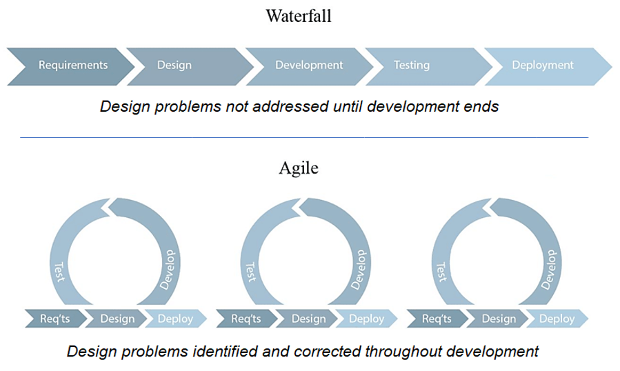
Over the past 20 years, a shift away from industrial-age-inspired waterfall development processes has occurred. In the past, all product functionality and construction requirements were documented upfront and were moved through a linear design and production process until finished products were finally ready for deployment. As new software and hardware products have become more complex, and as functionality has become more diverse, the waterfall development model has failed to properly accommodate changes in customer requirements and functionality.
Enter agile development. Any agile development process involves repeated design, build, and test iterations, which are executed throughout the product design process. Creating and performing important validation tests earlier in the design process, i.e., before a product design is finalized, allows functionality problems to be identified and addressed early. This reduces the extent of redesigns, both for new hardware and software products.
In agile electronics development, each iteration involves designing one or more portions of a product’s functionality, devising test cases, building prototypes, and testing functionality against design requirements. The traditional PCB prototyping process forces designers to put off tests until a product’s design is practically completed. This forces designers to rely on simulation tools throughout the design process and rely less on real test results.
3D printing changes this design, build, and test dynamic, as prototypes can be built and tested more often. This allows engineers to identify and triage required changes to a design, as well as quickly implement and test changes in customer requirements.
According to a 2018 survey, 62% of agile hardware designers stated they could benefit from implementing an additive manufacturing process for prototyping and manufacturing. When we look at the core ideas and processes in agile electronics development, we see that the primary benefit in this area is the ability to evaluate designs more often. 3D printing systems are unique in that a single, fully-functional prototype can be produced with a fixed lead time and immediately tested by a design team.
Agile electronics development requires multiple prototyping builds throughout the design phase.
The ability to build and test designs quickly is key to identifying functionality problems in complex electronic devices with diverse functionality and precise, signal, power, and usability requirements. Rather than waiting for a traditional prototyping run, designers can do this multiple times throughout the design process.
This allows designers to identify functionality problems, propose design changes, and quickly implement and test them with less impact on other portions of a complex system. The fixed lead time and cost provided by these systems means that a design with any level of complexity can be easily produced and tested in a matter of hours.
Innovative companies that want to experiment with unique PCB design choices can easily build and test their ideas when they work with an additive manufacturing system. The layer-by-layer deposition process used in additive manufacturing systems eliminates the constraints imposed by the traditional PCB manufacturing process.
Innovative design choices, such as non-orthogonal interconnect architecture, embedded components, and unique nonplanar board geometries can all be easily implemented and manufactured with fixed lead time and cost using the right additive manufacturing system. This reduces overall R&D time and helps innovative companies beat their competition to market.
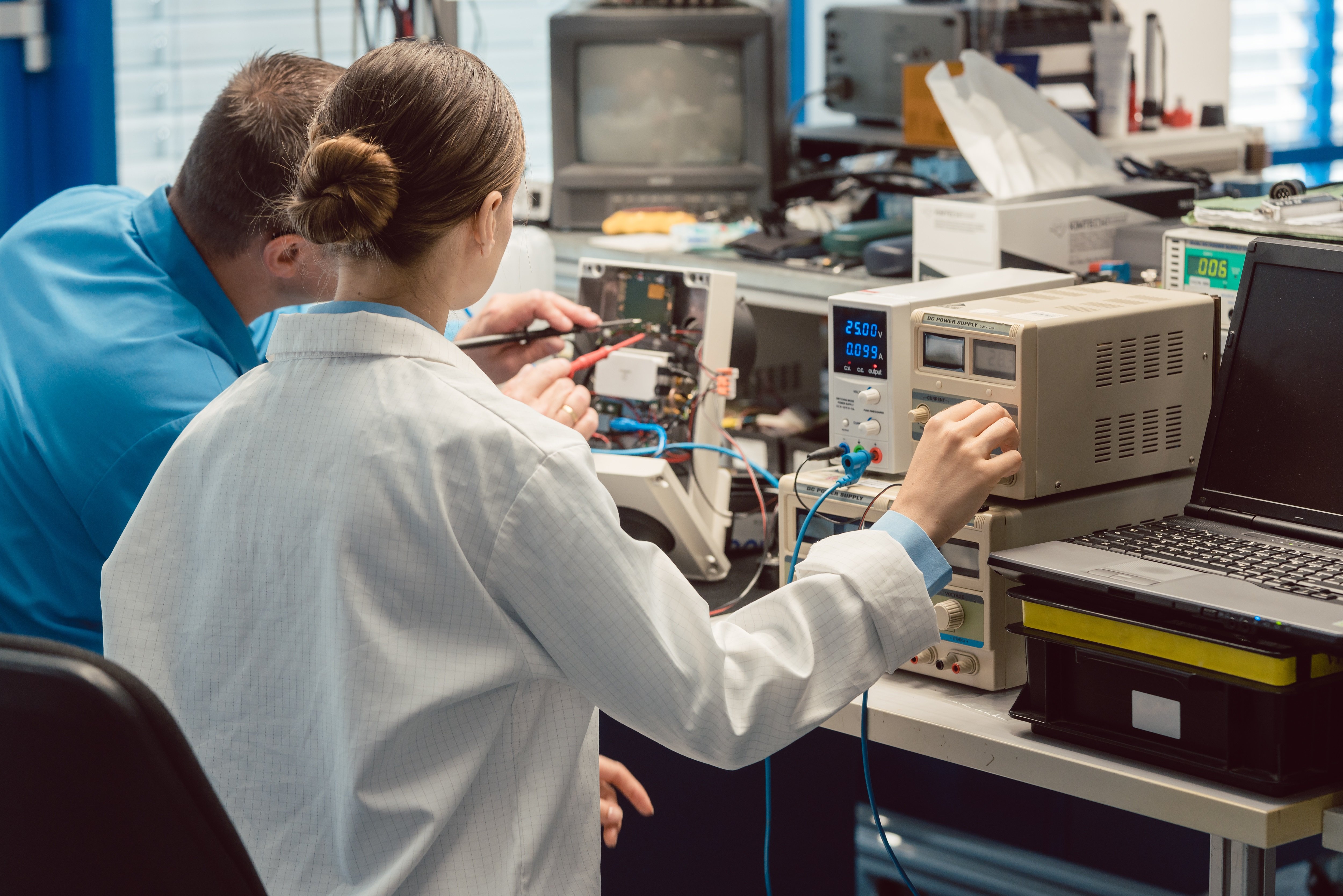
Engineers need to quickly fabricate and immediately test multiple prototypes in agile electronics development.
As more additive manufacturing systems become adapted for higher-volume digital manufacturing, newer, more complex products that are prototyped with these systems can then be produced at scale without changing the cost structure or fabrication time requirements. Currently, additive manufacturing systems for PCB prototyping and fabrication can be brought in-house, making them ideal for use in design, build, and test iterations in agile electronics development. As additive systems and processes are perfected, and as the range of useful materials expands, expect to see more agile electronics development made possible through with 3D printing technology.
The DragonFly LDM system from Nano Dimension is one of many digital manufacturing technologies that is set to revolutionize agile electronics development and full-scale PCB production. This system allows low- to medium-scale manufacturing of complex electronics with a planar or non-planar geometry, complex interconnect architecture, and embedded components. Read a case study or contact us today to learn more about the DragonFly LDM system.

Be informed of the future of additive manufacturing &
3D printed electronics

