3d printing
08 Jun 2020

Nano Dimension’s CEO Yoav Stern is talking about new trends to create PCBs

Oct 29, 2019

The semiconductor industry gets a lot of attention—and for good reason. Integrated circuits make technology possible, and these devices are built on the back of semiconductors.
Semiconductor manufacturing processes have come a long way since Robert Noyce invented the integrated circuit in 1959. With the rise of Industry 4.0 and the wide array of additive manufacturing processes, one naturally wonders whether the electronics industry will advance to 3D printing integrated circuits at full scale.
In this discussion, the question naturally arises: Why use additive manufacturing processes to produce integrated circuits? 3D printing is already being used to produce fully-functional PCBs with unique geometry, interconnect architecture, and various levels of component embedding. The ability to 3D print integrated circuits and other semiconductor devices directly into a PCB allows low-volume fabrication of highly specialized devices with unique form factor and capabilities.

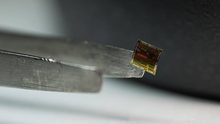
IC dies on a silicon wafer
Silicon, III-V, and II-VI semiconductor manufacturing processes are highly advanced and are used to produce integrated circuits with less than 10 nm gate sizes. Currently, the most advanced 3D printing processes provide near micron-level resolution and co-deposition of multiple materials.
Co-deposition is critical for 3D printing integrated circuits because conductors and semiconducting materials must be printed simultaneously. The resolution of the most advanced 3D printing systems must still improve before VLSI is possible. In addition to improving device performance, miniaturization will provide much lower power consumption for switching logic gates.
As an example of what is currently possible with 3D printing integrated circuits, researchers at the Air Force Research Laboratory and American Semiconductor recently 3D printed microcontroller SoCs from polymers on a flexible silicon substrate. These microcontroller units offer 7000x memory compared to other flexible integrated circuits at the time. Some envisioned applications include environmental or strain sensing, as well as munitions inventory monitoring.
A flexible microcontroller integrated circuit. This circuit was fabricated using polymers on silicon.
Currently, thin-film transistors (TFTs), diodes, LEDs, can be 3D printed from organic polymers with commercially available and experimental systems. The 3D-printed TFTs can have various contact/gate configurations and can easily be scaled horizontally and vertically. Polymers can be easily doped and functionalized, allowing their electronic and optical properties to be tuned to meet the demands of different devices.
Using polymers on a semiconductor wafer is a natural route to pursue 3D printing integrated circuits. Electrical contacts can already be deposited in an additive manner through a mask (i.e., thermal evaporation, PVD, or CVD), followed by deposition of semiconducting polymers and larger conductive tracks with a 3D printer. Their adaptability to low-temperature processes also makes them ideal for 3D printing integrated circuits directly on standard semiconductor wafers.
Other researchers are working on advancing additive manufacturing processes and materials to enable 3D printing integrated circuits. As an example, the University of Hamburg and Deutsches Elektronen-Synchrotron developed a 3D printing process that can enable the fabrication of integrated circuits. This process uses a mesh of ~20 nm silver nanowires as conductive elements and a thin film of polymer as an insulator or semiconducting material. This process is still in the research phase, but it illustrates how unique nanostructures can be used to fabricate semiconductor devices that rival silicon integrated circuits.
In any manufacturing process, the cost structure involved in manufacturing is an important driver of the price of a finished device. Integrated circuits succeed or fail based on the cost of the die on the wafer—when more dies can be placed on a single wafer, the costs per device decreases. The cost structure of integrated circuit manufacturing is responsible for the high costs of highly specialized, low-volume integrated circuits. An excellent example can be found in the defense industry, where the cost of a single FPGA for a complex system can reach tens of thousands of dollars.
The unique cost structure of 3D printed devices changes this economic dynamic. 3D printed integrated circuits do not need to be produced on a wafer and can even be manufactured individually. Because 3D printed devices can be produced with predictable fabrication time, and the cost structure is complexity agnostic, the costs involved in 3D printing electronics depends on the weight of the materials used. This makes 3D-printed integrated circuits highly cost competitive for low-volume production compared to devices produced on semiconductor wafers with standard processes.
Commercially available printers are becoming more advanced, and the range of materials useful with these systems is expanding. That being said, there are still some challenges in 3D printing integrated circuits with the same level of performance as integrated circuits on monolithic circuits. These challenges involve finding rigid semiconducting materials that can be adapted to a standard 3D printing process, optimizing these materials for different frequency bands, and bringing printing resolution closer to the nanometer level.
A lithographic process may aid in 3D printing integrated circuits with less than one-micron resolution.
The fact losses and parasitics can be optimized in a variety of polymers for specific frequency bands allows these materials to compete with GaN, which is currently the best option for fabricating RF integrated circuits and SoCs. GaN is currently used in the best SoCs for high-frequency radar modules, as well as in power amplifiers for microwave and mmWave signal chains. Polymers are already used to 3D print substrates for building flexible and nonplanar PCBs, so it is natural to extend these materials to integrated circuits and other semiconductor devices.
To increase the printing resolution, the additive manufacturing industry may need to devise a completely new printing process. Currently, inkjet 3D printing provides among the highest resolution features for 3D printing PCBs, but it remains to be seen if this process can be improved to provide resolution less than 1 micron.The future of 3D printing integrated circuits will likely adapt a photolithography process or functional self-assembly process to produce integrated circuits with competitive resolution.
Innovative companies that are interested in 3D printing integrated circuits and fully-functional PCBs need an additive manufacturing system designed for full-scale production of complex electronics. The DragonFly LDM system from Nano Dimension is ideal for in-house full-scale PCB fabrication of complex electronics with a planar or non-planar architecture. Designers can embed standard components and can experiment with 3D-printed integrated circuits. Read a case study or contact us today to learn more about the DragonFly LDM system.

Be informed of the future of additive manufacturing &
3D printed electronics

