3d printing
08 Jun 2020

Nano Dimension’s CEO Yoav Stern is talking about new trends to create PCBs

Oct 3, 2019
 Additive manufacturing and its core process of 3D printing are not always seen as being related. 3D printing is normally viewed as being used to fabricate plastic mechanical parts from 3D CAD models, but 3D printing is used in many industries for the fabrication of metal components. Groups of processes, like powder bed fusion (PBF), material jetting, inkjet printing, direct energy deposition (DED), and others, are useful for additive manufacturing a number of metal components directly from nanoparticles for various applications
Within PCB fabrication, additive manufacturing with nanoparticles is an extremely useful process for printing conductive pads, vias, and traces on an insulating substrate without being confined to planar substrates. Using nanoparticles for PCB fabrication in one of the aforementioned processes offers many advantages over less advanced methods, such as fused deposition modeling (FDM) with metal alloys on FR4 or another standard PCB substrate material.
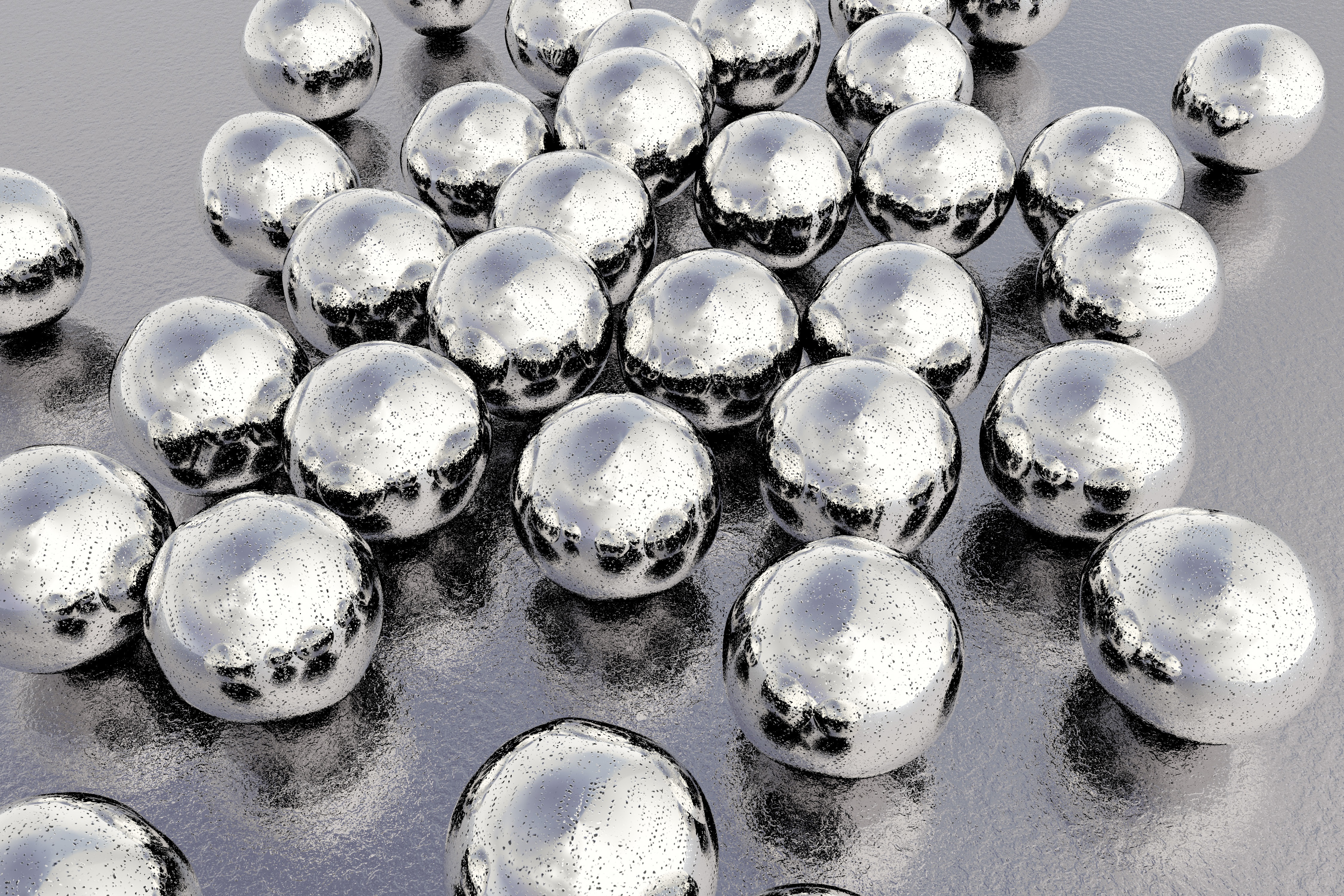
Silver is one common metal used in additive manufacturing with nanoparticles.
The use of traditional metal materials in 3D printing processes normally revolves around an extrusion process (such as FDM), which requires using a metal alloy with low melting temperature. Compared to noble metals like gold and silver, metal alloy filaments are cheap and easy to work with, but they tend to offer lower conductivity, making them less-than-ideal for electronic devices. In an extrusion process, the filament diameter and extrusion nozzle diameter are the primary factors that limit printing resolution.
As a result, PCBs fabricated with an extrusion process have thicker traces. This makes these devices appropriate for power electronic applications. Extrusion with these filament materials also requires a rigid substrate like FR4. This essentially limits designers to 3D printing on two-layer boards with thick traces, and without vias connecting each layer.
Conductive nanoparticles offer several advantages in 3D-printed PCBs and other electronic devices. The primary advantages are the range of useful materials (copper and silver are common) and higher printing resolution. DED, jetting, inkjet, and PBF processes (such as selective laser sintering) allow direct fabrication of PCBs with much smaller traces and fully functional electronic components. 3D-printed PCB traces that are formed with these processes have conductivity that is comparable to bulk material.
With the right combination of metal nanoparticles and insulating substrate material, fully-functional PCBs can be 3D printed with any of the above processes. Note that PBF and DED processes are difficult to adapt to a multi-material process, making it hard to co-deposit the substrate and conductor. Material jetting and inkjet printing are better options for co-deposition of conductors and substrates. The advantage of all four of these classes of 3D printing processes is that they can be adapted to more advanced materials, such as graphene, conductive polymers, and hybrid graphene-metal or hybrid polymer-metal materials.
Other innovators in the additive manufacturing space have successfully 3D printed conductive elements on PCBs using graphene and conductive polymers. These materials differ from using nanoparticles in several ways. These materials can compete with metal nanoparticles in terms of conductivity, mechanical strength, and flexibility in rigid-flex PCBs, and adaptability to different processes.
Conductive graphene filaments are available on the market and can be used within low-temperature (approximately 220 °C) deposition processes, such as FDM, filament DED, or another extrusion process. Although these extrusion processes have been used to 3D print simple PCBs, they are best used for mechanical components due to the limited resolution available with filaments.
Similar to metal nanoparticles, a better option is to use a hydrogel or ink suspension with graphene nanosheets in an inkjet or aerosol jetting process. Graphene oxide can also be used, followed by conversion to graphene nanosheets using a chemical reduction process (such as sonication via Hummers method, or exfoliation in water). Major chemical companies, like Sigma Aldrich, sell graphene oxide ink suspensions for use in various additive manufacturing systems. Carbon nanotube suspensions are also available for 3D printing composites using a jetting process, and filaments are available for use in FDM.
As an example of the potential offered by graphene inks and hybrid graphene-metal nanoparticle inks, researchers at the Institute of Sensors, Signals and Systems at Heriot-Watt University have shown that flexible electronic devices can be 3D printed using an inkjet process. In a more recent publication in Advanced Functional Materials, researchers presented several single-layer and multilayer electronic devices that were fabricated using a conformal screen printing process from graphene inks.
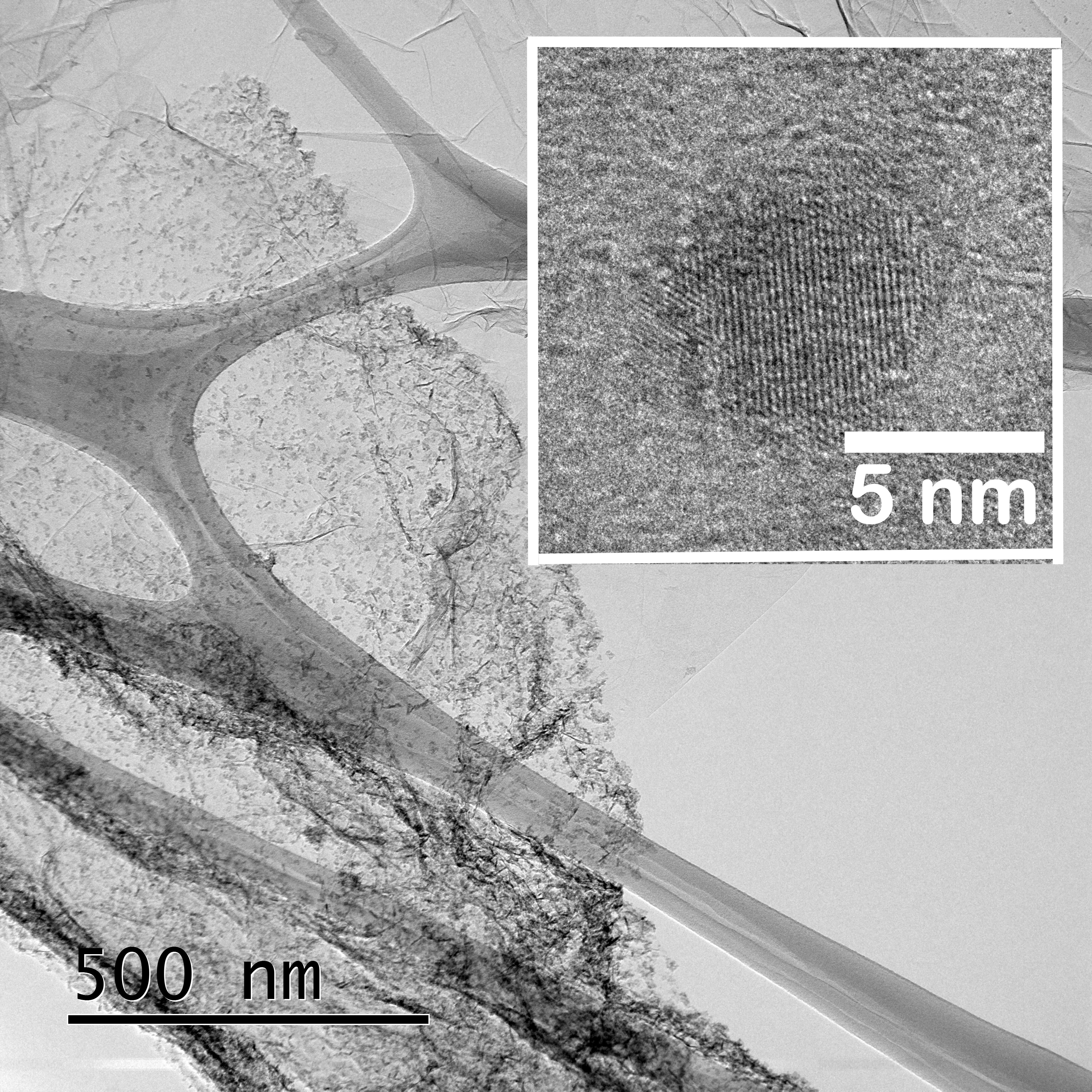
TEM image of graphene oxide nanosheets that were hybridized with iron oxide carbon nanoparticles.
Polymers have a broad range of electrical properties, ranging from insulating to conductive, and can be used in low-temperature processes. For example, filaments of solid conductive polymers can be used in an extrusion process (such as FDM). Similarly, conductive polymer nanoparticles can be deposited with a jetting technique, both from solution and suspension. Depositing from solution is preferable as it eliminates a subsequent sintering step. Deposition from solution and suspension both require a polymerization step to create a continuous film after deposition.
As the electrical and optical properties of polymers vary widely and they can be tuned through functionalization, these materials are ideal for direct 3D printing of semiconductor devices. A group of Chinese researchers recently presented piezoelectric elements and transparent electrodes that were 3D printed from poly(3,4-ethylenedioxythiophene) (PEDOT) nanoparticles, illustrating potential uses in photonic devices directly on PCBs. Conductive polymer nanoparticles can also be used as traces in flex-PCBs on a flexible polymer substrate (e.g., polyimide).
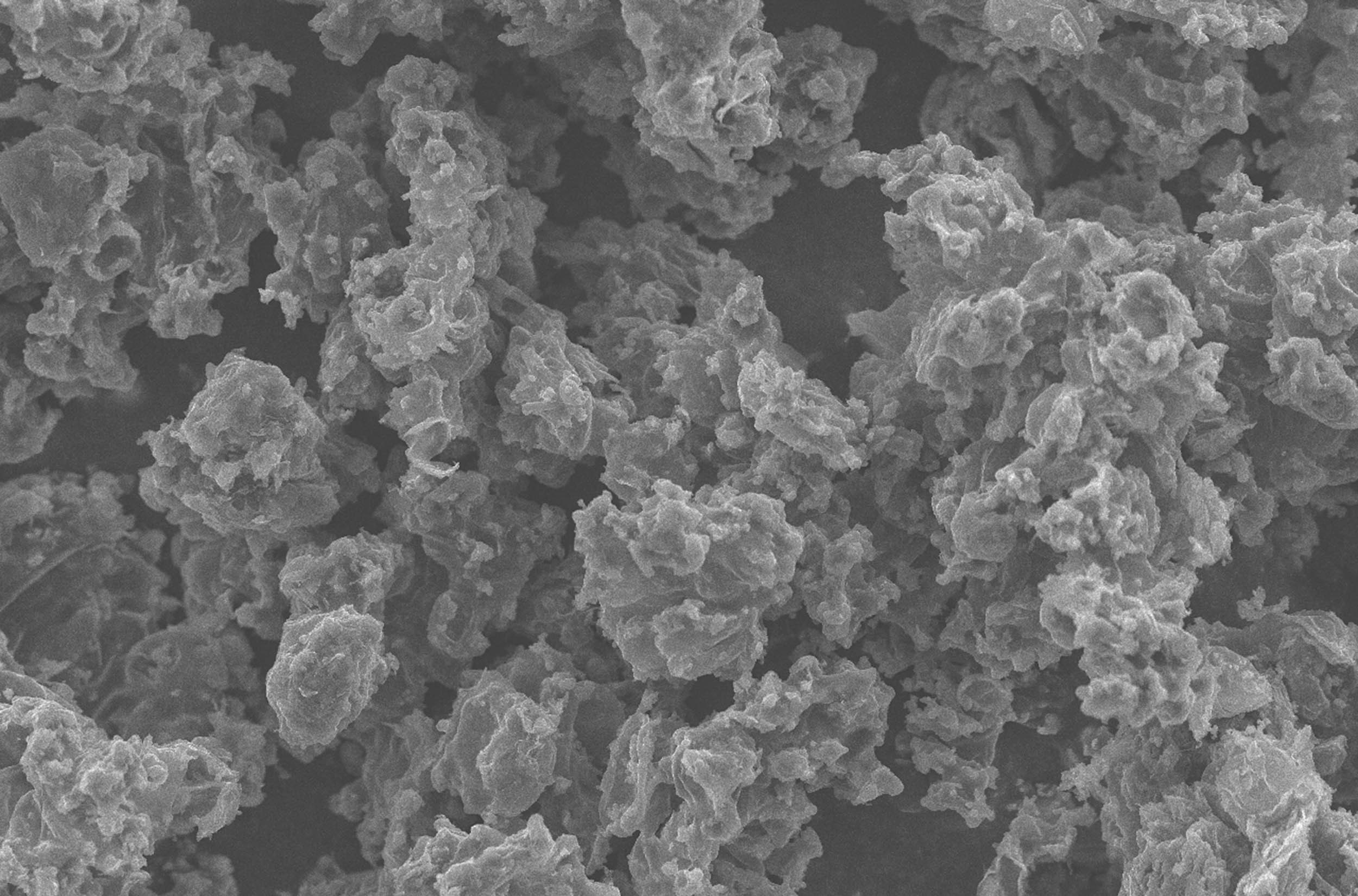
SEM image of conductive oxidized polythiophene nanoparticles.
In their nanoparticle form, the materials discussed here can be easily functionalized by adding organic functional groups, allowing the optical and electrical material properties to be tuned with relatively simple chemical processes in solution/suspension. Engineers and scientists looking for more guidance on material selection and functionalization in additive manufacturing with nanoparticles can find excellent guidance from a recent review in MDPI. They’ve provided a more comprehensive overview of the use of additive manufacturing with nanoparticles than we can provide here.
At present, much of the research in the field and commercial systems focus on the deposition of a single material during the fabrication process. As the additive manufacturing space sees continued innovation, expect to see more systems that can co-deposit multiple materials for different applications. Within the realm of electronics, systems, and processes that allow co-deposition of insulating and conductive materials provide superior throughput compared to other processes.
An inkjet process is ideal for additive manufacturing of electronics with conductive nanoparticle inks as it offers high resolution, no material waste, and fixed fabrication time per unit weight of deposited material. The right additive manufacturing system will allow co-deposition of conductive and insulating inks, making it ideal for 3D printing fully-functional PCBs. The layer-by-layer printing process allows the fabrication of unique multilayer boards with nearly any interconnect architecture, embedded components, and any geometry.
If you’re an electronics engineer, additive manufacturing with nanoparticles and other advanced materials requires a system that adapts sophisticated deposition processes for PCB fabrication. Whether you are fabricating prototypes or planning for full-scale production, the DragonFly LDM additive manufacturing system from Nano Dimension is ideal for in-house fabrication of complex electronics with a planar or non-planar architecture. Read a case study or contact us today if you’re interested in learning more about the DragonFly LDM system.

Be informed of the future of additive manufacturing &
3D printed electronics

