
Apr 20, 2022
ProtoSpace Uses AME To Print A Custom Multilayer Bandpass Filter

CLIENT
The ProtoSpace of University of Technology Sydney (UTS) is Australia’s most advanced additive manufacturing facility located in the heart of Sydney. UTS ProtoSpace provides access to advanced 3D printing and scanning technologies along with specialized technical support, linked education, and engagement opportunities. Dr. Yang Yang is a group leader of Millimetre-Wave Integrated Circuits and Antennas at UTS Tech Lab and currently a principal supervisor of five PhD students.
CHALLENGE
The upcoming wireless ecosystem will enable billions of high-speed wireless devices in a dynamic environment. Undoubtedly, highly-integrated circuits built through Additively Manufactured Electronics (AME) technology, operating at millimeter-wave bands and packaged on mobile devices, will enable a new era of 5G IoT. However, the development of AME 5G devices is still in its infancy with several unique challenges still needing to be addressed.
First is the high cost and long cycle of production for mm-wave circuit-in-Package (CiP), which makes proof-of-concept prototyping difficult especially for start-ups and small businesses. Secondly, circuit miniaturization in wireless mobile devices plays a significant role in 5G IoT communications and sensing applications. There is still the question of how best to integrate and miniaturize packaged microwave circuits in small form factors without losing critical performance. Although the multi-metal-layer technique has an outstanding advantage, it is still a challenge to realize the fabrication of seamless multi-metal-layer in a single substrate with 3D printing.
THE SOLUTION
Based on the proof-of-concept obtained from a pilot project between UTS and Nano Dimension, Dr. Yang and his team discovered a unique AME solution for 5G mm-wave circuit-in-package (CiP) designs by delivering single-substrate multiple conductive layers with customized package profiles without risking confidentiality and intellectual property security.
The AME solution is utilized to fabricate multi-metal-layer CiP devices seamlessly in a single substrate. Most importantly, the prototyping cost is far cheaper than traditional methods, which requires a minimum panel order at an exaggerated price, making the realization of initial proof-of-concept more difficult.
THE RESULTS
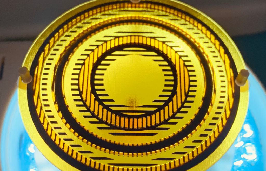
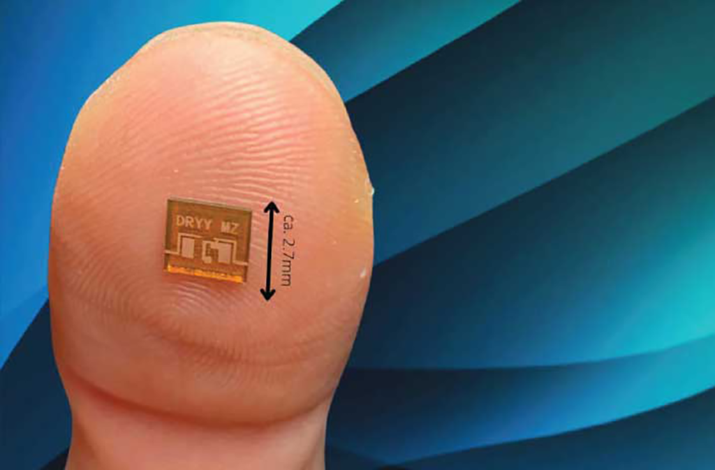
This paper presented an additively manufactured bandpass filter (BPF) based on a second-order stub-loaded resonator consisting of multi-metal layer components. The proposed BPF is fabricated by a low-temperature (140°) AME solution that can fabricate conductive and dielectric materials simultaneously with multi-metal-layer and flexible interlayer distance. By reducing the interlayer distance, constant inductance and capacitance can be realized in smaller sizes, which helps to achieve device minimization.
Taking advantage of this inkjet printing technology, a second-order multi-metal layer resonator is proposed. To understand the principle of the BPF, an equivalent circuit with odd- and even-mode analysis is demonstrated. For verification, the frequency response of the circuit’s mathematical model is calculated to compare with the electromagnetic simulation results. Good agreement can be achieved among the calculated, simulated, and measured results.
The proposed BPF is designed at 12.25GHz with a bandwidth of 40.8% and a compact size of 2.7 mm × 1.425 mm × 0.585 mm or 0.186λg × 0.098λg× 0.040λg, which is suitable for circuit-in-package applications in television programs, radar detection and satellite communications.
KEY ADVANTAGES
The DragonFly® system is the industry’s only comprehensive additive manufacturing platform. It provides significant advantages in electronic circuits and antennas that are set to be widely used in 5G IoT electronics. The printer is helping start-ups and small- and medium-sized businesses protect their IP and prototype fast at low cost.
This project featured:
• Solutions that enable miniaturization of microwave and millimeter-wave package circuits for easy integration into mobile terminal systems.
• Single-substrate multiple conductive layers CiP.
• Constant inductance and capacitance that can be realized in smaller sizes by reducing the interlayer distance.
To read the technical research paper in full, and see “Compact Multilayer Bandpass Filter Using Low-Temperature Additively Manufacturing Solution” published by IEEE.

Stay Updated
Be informed of the future of additive manufacturing &
3D printed electronics