
A Brief Introduction to Additively Manufactured Electronics
Learn about AME, the emerging model of electronics design and production.

Feb 9, 2023
Today’s electronics world is fast-paced, competitive, and ever evolving, but it faces obstacles that are stunting its otherwise boundaryless potential such as the limitations related to the miniaturizing of components and electronics design.
As the year-over-year miniaturizing rate of components declines significantly, industry needs to look for size and weight reduction in the electronics systems holding these components. And this is where “System in Package,” or SiP, can be an answer.
Understanding SiP and its Challenges
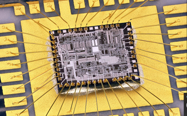
SiP is several integrated circuits that are bundled together on a carrier by utilizing various interconnect methods. Think of a printed circuit board, or PCB, but at a much smaller scale. The SiP performs all or most of the functions of an electronic system and is typically used inside myriad electronic devices from high-tech defense systems to intricate medical devices to mobile phones.
Companies manufacturing SiPs prefer to run their machines for high-volume to maximize production and thruput, nourishing the most attractive accounts, while an extensive line of small and medium enterprises line up and wait and/or pay a premium to receive SiP fabrication services.
Couple this with other supply chain challenges and R&D becomes a long, drawn-out process – often discouraging ingenuity and iteration. This is especially impactful to companies involved in manufacturing high-variety and small volume.

The current SiP process planning, system design, and die implementation is a complex, multi-step process, each with its own challenges and potential for delay. The result is a long, unpredictable R&D cycle – likely requiring several timely cycles to produce a single prototype.
What Spawned QuickSiP
Nano Dimension has embarked on a quest to create a more dependable, efficient, and prevalent way to design and manufacture SiP devices using AME, or Additively Manufactured Electronics – an initiative dubbed QuickSip. And the results of its extensive beta testing thus far are encouraging and exciting.
Nano Dimension is the pioneer in the AME space with the introduction of its DragonFly IV® system, which uses digital files and 3D simultaneous printing of dielectric and conductive materials to produce high-performance, multilayered electronic parts.
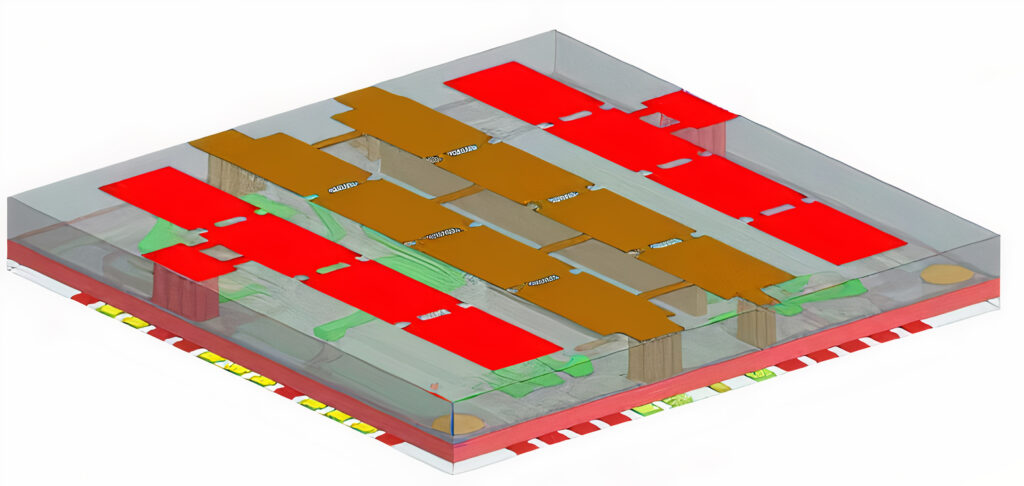
A technical team at Nano Dimension is collaborating with an external partner on QuickSiP to demonstrate how SiP structures can be produced using AME technology, including generating detailed connectors and pinpoint-precise cavities for mounting the remaining components (integrated circuits and microprocessors cannot be additively manufactured) with no need for drilling.
In contrast to traditional approaches, QuickSiP intends to avoid wire-bonding processes. Instead, the connection of the bare die to the AME carrier structure is realized with suitable AME printing processes.
QuickSiP would allow for prototypes in a fraction of the time and quick iteration of new electronic products. For academic labs, this would give immediate one-offs for the design of experiments. For commercial manufacturers, this could mean shorter development timelines to bring quality products to market faster than the competition. The SiP production market is projected to have an 8% compound annual growth rate until 2030.

Nano Dimension believes that QuickSiP can reduce R&D time from 12 months to 2 months, allow for both significant weight and size reductions, and can create a variety of low-volume SIPs. Multilayers of SiP are possible that would create even more complex and function designs to be printed.
QuickSiP using DragonFly IV®
After extensive testing, the overall dimensions of the QuickSiP package are 13.2×13.2×1.5mm with minimum pad size on die of 70um (approximately 60% of the market is circa 70um). The components to be placed in the package are 1 MMIC 4W X-band die (QPA1022D), 6 resistors, 3 capacitors and 2 MOSFET dies.
The team overcame challenges related to registration (removing and bringing back the printed structures), creating a flat surface on top of printed circuit structures, process automation, introducing flip-chip as an additional option, materials adhesion, and rapid testing of samples.
Split Assembly Process design was split into 3 parts:
There is also opportunity to further automate and introduce a flip-chip assembly process that could enable integration with a pick-and-place machine.
The Nano Dimension team is encouraged at what the DragonFly IV®-generated QuickSiP has demonstrated, and eager to see how this technology evolves and the positive impact potential for a broad spectrum of products and industries.

Be informed of the future of additive manufacturing &
3D printed electronics