Products
DragonFly IV+
Build, Test, and Iterate Electronics in a Single Day
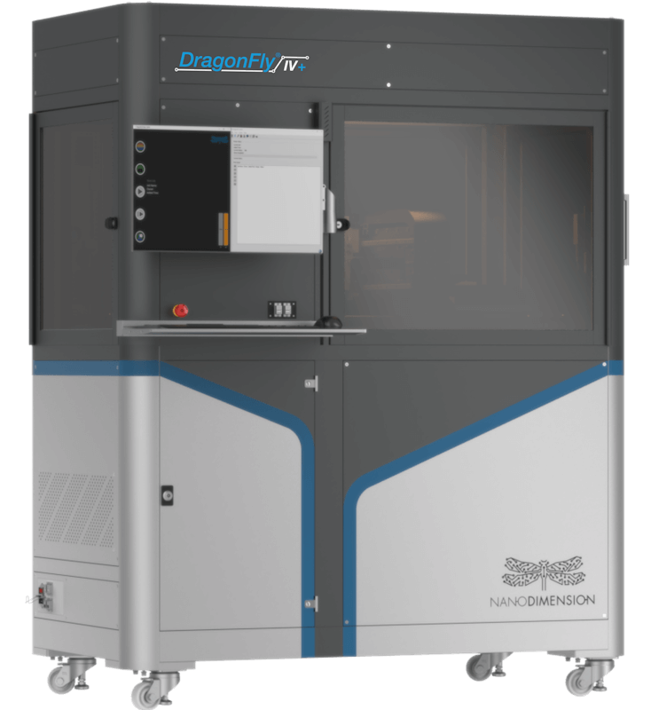
A multi-material, multi-layer 3D printer that generates entire circuits in one step – including substrate, conductive traces, and passive components
____________________________________________________________________________________________
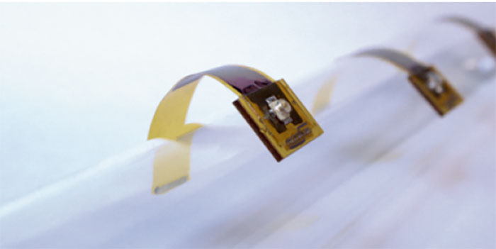
Design Flexibility Beyond Traditional Boundaries
A completely new way to build electronics

Freedom in Three Dimensions
Layouts can now make connections in any 3D direction

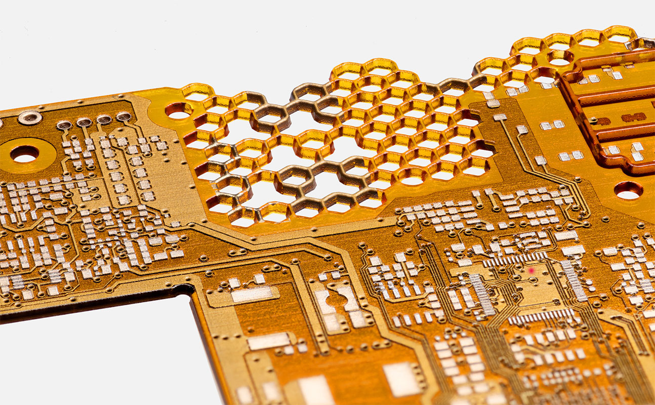
Novel Form Factors
FLIGHT software allows for new shapes in electro-mechanical CAD
Transformational Processes
Highly agile design and production in days, not weeks or months
Digital End-to-End Execution
Additively Manufactured Electronics (AME) removes human error and lengthy manual operations
Cleaner Methods
3D printing eliminates toxic chemical waste and dramatically reduces energy consumption
Generate Devices in House
Turn ideas into fully functional circuits within hours
Protect Your IP
Keep ideas confidential within your organization
High Performance
Component electrical performance is comparable to traditional devices
Applications

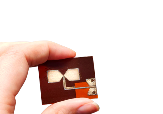
3D Printed Bow Tie Antenna
The DragonFly™ System can print antennas and arrays using conductive nano-particle silver and dielectric inks.
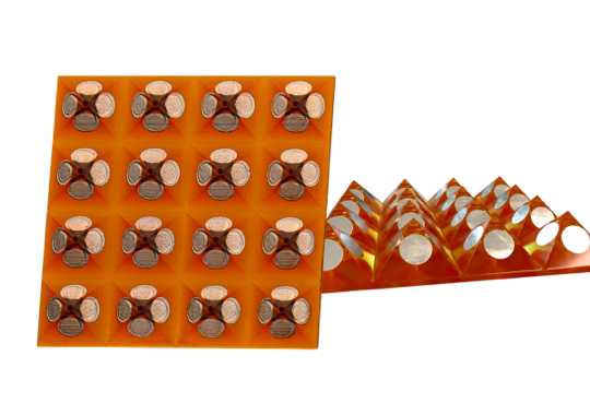
Sphere Phased Array Antenna
5G technology demands improved performance, functionality, and increased miniaturization.
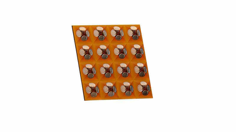
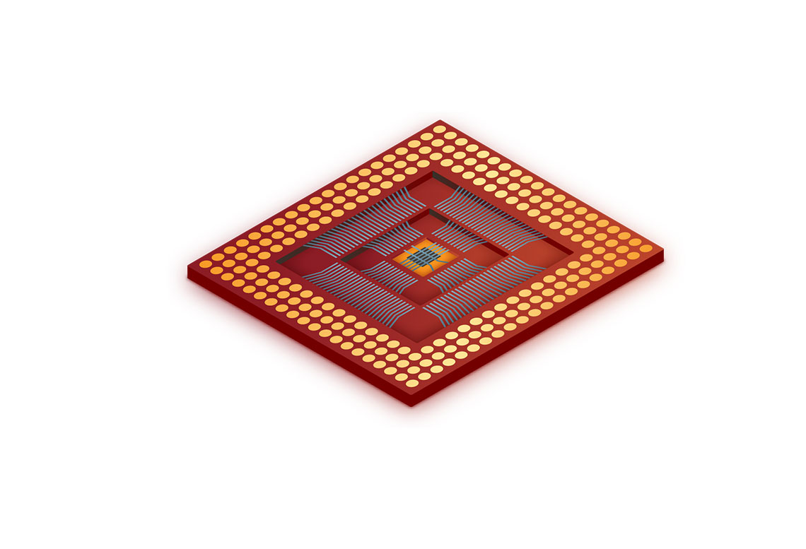
Vertically-stacked Integrated Circuits
Stacked ICs in an AME structure have a higher circuitry density than traditional PCBs.
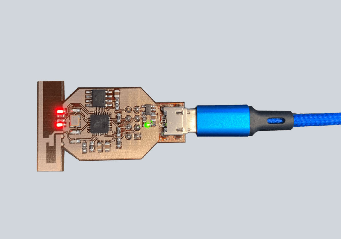
IOT / WIFI Access Point
This IoT/WiFi access point achieved a tested data transmission and reception accuracy of over 99%.
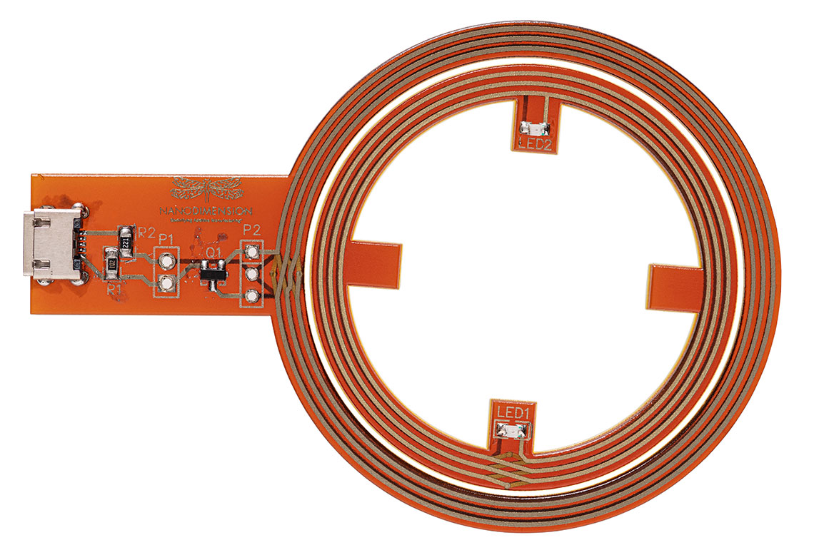
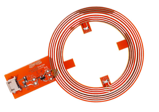
3D Printed Inductor for Wireless Charger
The DragonFly™ 3D printer created a new class of inductor leveraging new 3D circuit layout
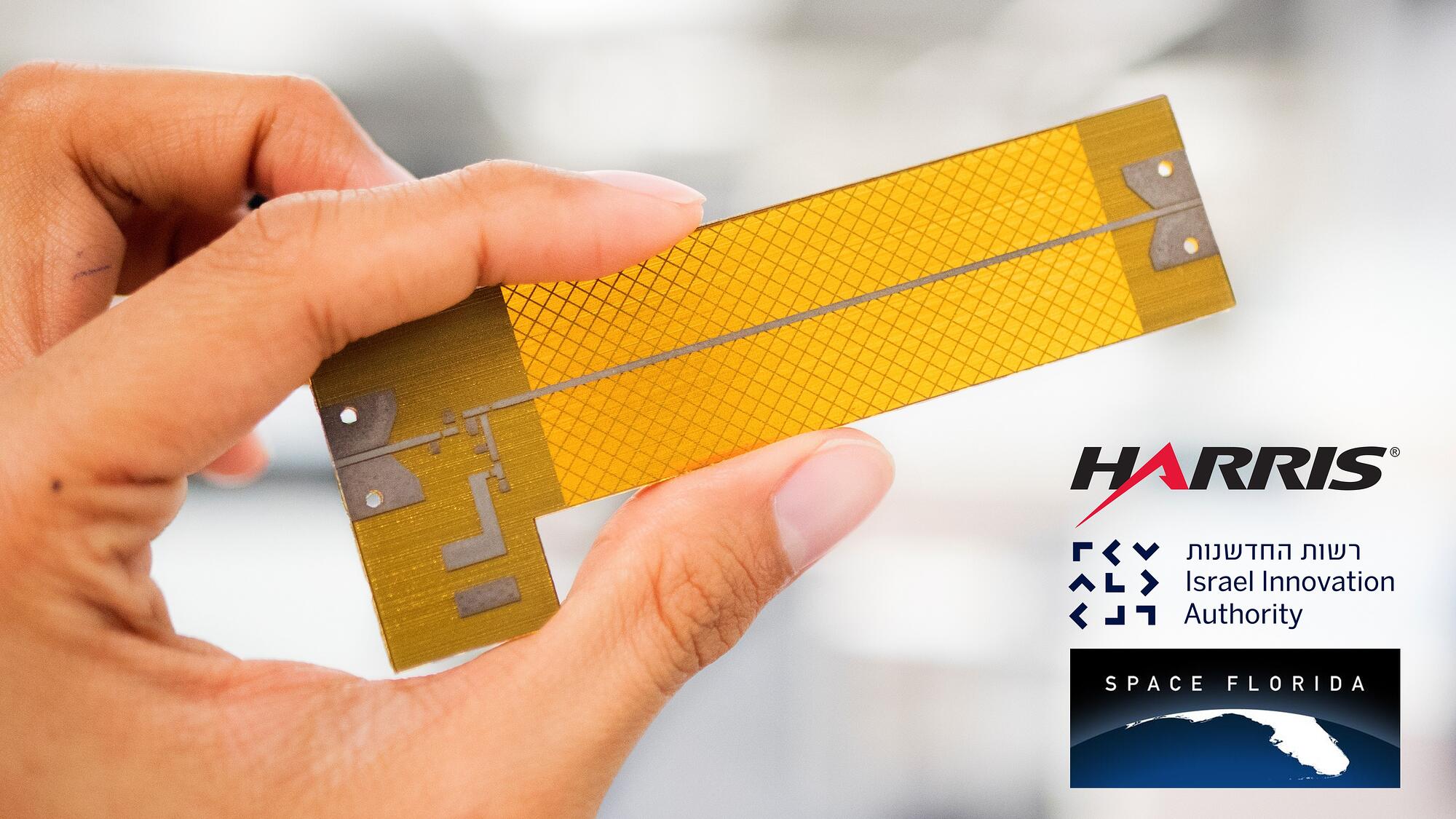
3D-Printed RF Amplifier
L3 Harris Corporation and Nano Dimension collaborated to use of additive manufacturing for radio frequency (RF) circuits in RF systems.
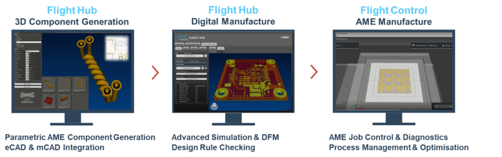
Pair with our FLIGHT software
DragonFly IV+ Tech Specs and Capabilities
- Dimensions
1,400mm x 800mm x 1,800mm - Weight
520kg, (1,150lbs) - Power Supply*
230 VAC, 20A, 50–60Hz - Network Connectivity
Ethernet TCP/IP 10/100/1000 - Operational Humidity
Above 35% non-condensing - Operational Temperature
18°C (64°F) to 25°C (77°F) - Regulatory Compliance
UL, CE, FCC - Deposition Technology
Piezo drop-on-demand inkjet - Number of Printheads
2, one for each ink: conductive and dielectric - Software
FLIGHT HUB Software Suite (Design, Verification, Pre-Production)
- Build Volume
160mm x 160mm x 1.7mm - Inks
Optimized silver nano particles and dielectric inks - Supported File Formats
All major eCAD and mCAD Software, ODB++, Gerber & Excellon, STL, OBJ - Resolution
18 µm (x), 18 µm (y), 10 µm (z) - Min. Line/Space
100 μm traces/ 150 μm spacing - Min. BGA Pitch
400 μm - Min. Via
200 µm - Min. Dielectric Layer Thickness
5.4 μm - Min. Conductive Layer Thickness
1.3 μm - Conductivity (Relative to Copper)
100 um – 125 μm traces width: 29% ± 4%
| Trace width ≥ 150 μm: 33% ± 4% - Dielectric Constant (Dk) @ 2 GHz/15 GHz
2.98 / 2.92 - Tangential Loss (Df) @ 2 GHz/15 GHz
0.02 / 0.02
Specifications
Capabilities
* Must use UPS (Uninterruptible Power Supply)
This data represents typical tested values at a controlled environment. Material properties can vary with part geometry, print orientation, print settings, environmental conditions and additional variables. To learn more about specific testing conditions, please contact a Nano Dimension representative. Specific performance of customer parts should be tested in accordance with customer’s specifications.
The above detailed data was tested, measured, or calculated using standard methods based on, inter alia, ASTM and IPC standards and are subject to change without notice. To the fullest extent permissible pursuant to applicable law, Nano Dimension (including any affiliate thereof) disclaims all warranties of any kind, express or implied. The above detailed data should not be used to establish design, quality control, or specification limits, and is not intended to substitute customer’s own testing to determine suitability for a particular application.
DragonFly IV in Action Spotlight