Services
Support
Nano Dimension Support
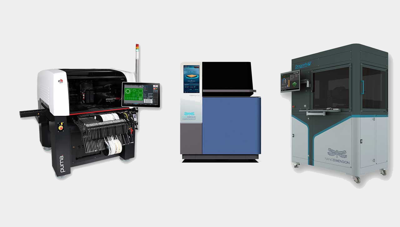
Find contact details for support of Nano Dimension and Essemtec product lines
Services Hotline
![]()
DragonFly & Fabrica Support, USA
Contact our Nano Dimension Service Hotline for questions on pricing, shipping and services.
Hours: Mon-Fri, 10am-5pm (ET)
Phone: +1 408 824 8242
Email: support@nano-di.com
Essemtec USA Support

Contact our Essemtec Service Hotline for questions on pricing, shipping and services.
Hours: Mon-Fri 10am-5pm (ET)
Phone: +1 (856) 218 1131
Business matters: sales-usa@essemtec.com
Technical support: service-usa@essemtec.com
Spare parts: spares-usa@essemtec.com
Order processing: orders-usa@essemtec.com
Invoices and payments: finance-usa@essemtec.com
Visit the Customer Learning Center
Technical sessions, manuals, how-to guides and more (Login required)
Talk to a Sales Expert
Visit our Contact Us Page